7C1325B-100 データシートの表示(PDF) - Cypress Semiconductor
部品番号
コンポーネント説明
メーカー
7C1325B-100 Datasheet PDF : 17 Pages
| |||
CY7C1325B
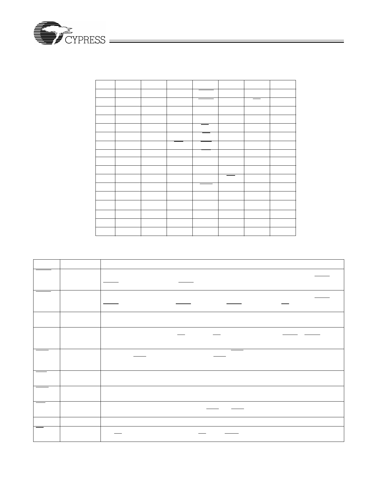
Pin Configurations (continued)
119-Ball BGA
1
2
3
4
5
6
7
A
VDDQ
A
A
ADSP
A
A
VDDQ
B
NC
CE2
A
ADSC
A
CE3
NC
C
NC
A
A
VDD
A
A
NC
D
DQb
NC
VSS
NC
VSS
DQPa
NC
E
NC
DQb
VSS
CE1
VSS
NC
DQa
F
VDDQ
NC
VSS
OE
VSS
DQa
VDDQ
G
NC
DQb
BWb
ADV
Vss
NC
DQa
H
DQb
NC
VSS
GW
VSS
DQa
NC
J
VDDQ
VDD
NC
VDD
NC
VDD
VDDQ
K
NC
DQb
VSS
CLK
VSS
NC
DQa
L
DQb
NC
Vss
NC
BWa
DQa
NC
M
VDDQ
DQb
VSS
BWE
VSS
NC
VDDQ
N
DQb
NC
VSS
A1
VSS
DQa
NC
P
NC
DQPb
VSS
A0
VSS
NC
DQa
R
NC
A
MODE
VDD
VSS
A
NC
T
NC
A
A
NC
A
A
ZZ
U
VDDQ
NC
NC
NC
NC
NC
VDDQ
Pin Descriptions
Name
ADSC
ADSP
A[1:0]
A[17:2]
BWS[1:0]
ADV
BWE
GW
CLK
CE1
I/O
Input-
Synchronous
Input-
Synchronous
Input-
Synchronous
Input-
Synchronous
Input-
Synchronous
Input-
Synchronous
Input-
Synchronous
Input-
Synchronous
Input-Clock
Input-
Synchronous
Description
Address Strobe from Controller, sampled on the rising edge of CLK. When asserted LOW, A[17:0]
is captured in the address registers. A[1:0] are also loaded into the burst counter. When ADSP and
ADSC are both asserted, only ADSP is recognized.
Address Strobe from Processor, sampled on the rising edge of CLK. When asserted LOW, A[17:0]
is captured in the address registers. A[1:0] are also loaded into the burst counter. When ADSP and
ADSC are both asserted, only ADSP is recognized. ASDP is ignored when CE1 is deasserted HIGH.
A1, A0 address inputs, These inputs feed the on-chip burst counter as the LSBs as well as being
used to access a particular memory location in the memory array.
Address Inputs used in conjunction with A[1:0] to select one of the 256K address locations. Sampled
at the rising edge of the CLK, if CE1, CE2, and CE3 are sampled active, and ADSP or ADSC is active
LOW.
Byte Write Select Inputs, active LOW. Qualified with BWE to conduct byte writes. Sampled on the
rising edge. BWS0 controls DQ[7:0] and DP0, BWS1 controls DQ[15:8] and DP1. See Write Cycle
Descriptions table for further details.
Advance input used to advance the on-chip address counter. When LOW the internal burst counter
is advanced in a burst sequence. The burst sequence is selected using the MODE input.
Byte Write Enable Input, active LOW. Sampled on the rising edge of CLK. This signal must be
asserted LOW to conduct a byte write.
Global Write Input, active LOW. Sampled on the rising edge of CLK. This signal is used to conduct
a global write, independent of the state of BWE and BWS[1:0]. Global writes override byte writes.
Clock input. Used to capture all synchronous inputs to the device.
Chip Enable 1 Input, active LOW. Sampled on the rising edge of CLK. Used in conjunction with CE2
and CE3 to select/deselect the device. CE1 gates ADSP.
3
Share Link: 