LHF32K10 „Éá„Éľ„āŅ„ā∑„Éľ„Éą„ĀģŤ°®Á§ļÔľąPDFÔľČ - Sharp Electronics
ťÉ®ŚďĀÁē™ŚŹ∑
„ā≥„É≥„ÉĚ„Éľ„Éć„É≥„ÉąŤ™¨śėé
„É°„Éľ„āę„Éľ
LHF32K10 Datasheet PDF : 61 Pages
| |||
sharp
LHF32K10
10
Mode
Read
Output Disable
Standby
Deep Power-Down
Read Identifier
Codes
Query
Write
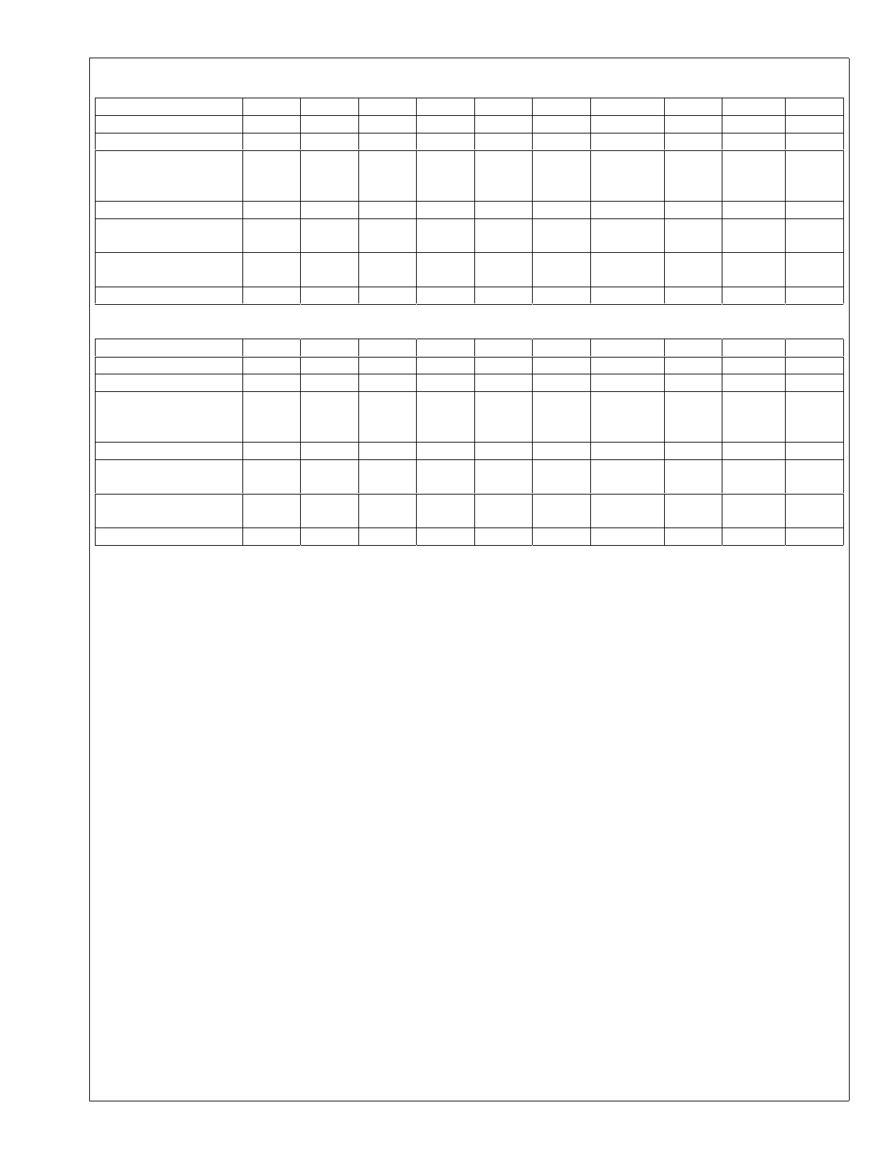
Table 3. Bus Operations(BYTE#=VIH)
Notes RP# CE0# CE1# OE# WE# Address VPP
1,2,3,9 VIH
VIL
VIL
VIL
VIH
X
X
3
VIH
VIL
VIL
VIH
VIH
X
X
VIH
VIH
3
VIH
VIH
VIL
X
X
X
X
VIL
VIH
4
VIL
X
X
X
X
X
X
9
VIH
VIL
VIL
VIL
VIH
See
Figure 4
X
9
VIH
VIL
VIL
VIL
VIH
See Table
7~11
X
3,7,8,9 VIH
VIL
VIL
VIH
VIL
X
X
DQ0-15
DOUT
High Z
STS
X
X
High Z X
High Z High Z
Note 5 High Z
Note 6 High Z
DIN
X
Table 3.1. Bus Operations(BYTE#=VIL)
Mode
Notes RP# CE0# CE1# OE# WE# Address VPP DQ0-7 STS
Read
1,2,3,9 VIH
VIL
VIL
VIL
VIH
X
X
DOUT
X
Output Disable
3
VIH
VIL
VIL
VIH
VIH
X
X High Z X
VIH
VIH
Standby
3
VIH
VIH
VIL
X
X
X
X High Z X
VIL
VIH
Deep Power-Down
4
VIL
X
X
X
X
X
X High Z High Z
Read Identifier
Codes
9
VIH
VIL
VIL
VIL
VIH
See
Figure 4
X
Note 5 High Z
Query
9
VIH
VIL
VIL
VIL
VIH
See Table
7~11
X
Note 6 High Z
Write
NOTES:
3,7,8,9 VIH
VIL
VIL
VIH
VIL
X
X
DIN
X
1. Refer to DC Characteristics. When VPP‚ȧVPPLK, memory contents can be read, but not altered.
2. X can be VIL or VIH for control pins and addresses, and VPPLK or VPPH1 for VPP. See DC Characteristics for
VPPLK and VPPH1 voltages.
3. STS is VOL (if configured to RY/BY# mode) when the WSM is executing internal block erase, full chip erase,
(multi) word/byte write or block lock-bit configuration algorithms. It is floated during when the WSM is not busy,
in block erase suspend mode with (multi) word/byte write inactive, (multi) word/byte write suspend mode, or
deep power-down mode.
4. RP# at GND¬Ī0.2V ensures the lowest deep power-down current.
5. See Section 4.2 for read identifier code data.
6. See Section 4.5 for query data.
7. Command writes involving block erase, full chip erase, (multi) word/byte write or block lock-bit configuration are
reliably executed when VPP=VPPH1 and VCC=VCC1/2.
8. Refer to Table 4 for valid DIN during a write operation.
9. Don’t use the timing both OE# and WE# are VIL.
Rev. 1.55
Share Link: 