HV430WG データシートの表示(PDF) - Supertex Inc
部品番号
コンポーネント説明
メーカー
HV430WG Datasheet PDF : 8 Pages
| |||
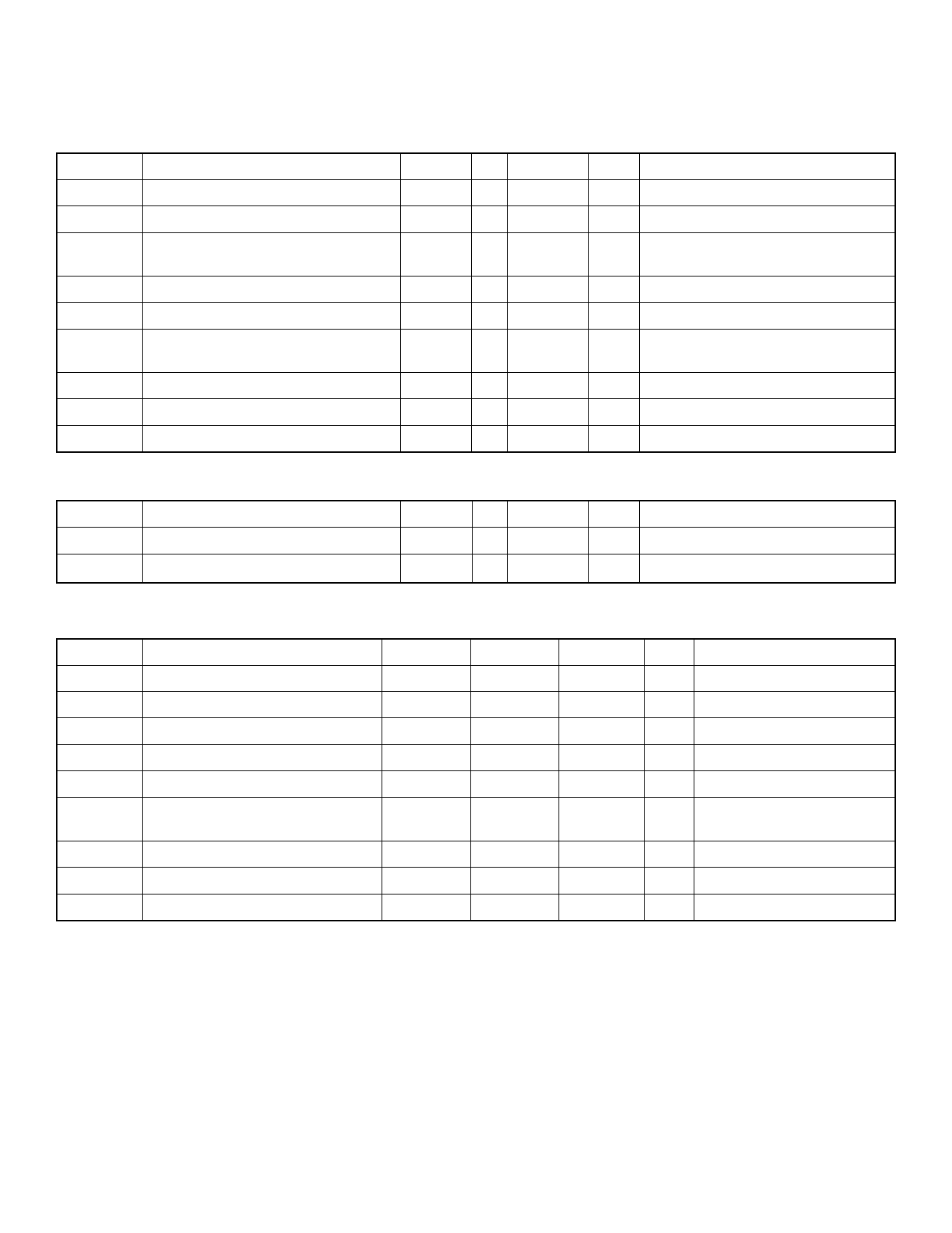
Electrical Characteristics
(Over operating supply voltage unless otherwise specified, TA = -40°C to +85°C.)
External Supplies
Symbol
Parameter
VPP1
High voltage positive supply
IPP1Q
VPP quiescent current
IPP1
VPP operating current
Min Typ
50
250
Max
200
500
2.0
VNN1
INN1Q
INN1
High voltage negative supply
VNN1 quiescent current
VNN1 operating current
VPP1-325
-50
250 500
1.0
VDD
Logic supply voltage
IDDQ
VDD quiescent current
IDD
VDD operating current
4.50
300
5.50
400
1.0
HV430
Unit
V
µA
mA
V
µA
mA
V
µA
mA
Conditions
PIN=NIN=0V
No load
VOUTP and VOUTN switching at 100kHz
PIN=NIN=0V, RDB =18kΩ
No load
VOUTP and VOUTN switching at 100kHz
PIN=NIN=0V, RDB =18kΩ
PIN=NIN=100kHz, RDB =18kΩ
Internal Supplies
Symbol
Parameter
Min Typ
VPP2
Positive linear regulator output voltage VPP1-16
VNN2
Negative linear regulator output voltage VNN1+10
Max
VPP1-10
VNN1+14
Unit
V
V
Conditions
Positive High Voltage Output
Symbol
Parameter
VPgate
Output voltage swing
RsourceP VPgate source resistance
RsinkP
VPgate sink resistance
triseP
VPgate rise time
tfallP
VPgate fall time
tpwp(min)
VPgate minimum pulse width
(internally limited)
tdelayP
PIN to Pgate delay time
VPsen
VPgate current sense voltage
tshortP
VPgate current sense off time
Min
VPP2
100
VPP1-0.85
Typ
150
VPP1-1.0
Max
VPP1
12.5
12.5
50
50
Unit
Conditions
V No load on VPgate
Ω IOUT=80mA
Ω IOUT=-80mA
ns Cload=1.4nF
ns Cload=1.4nF
200
300
VPP1-1.15
150
ns
ns mode=1
V
ns
2
Share Link: 