HV430 データシートの表示(PDF) - Supertex Inc
部品番号
コンポーネント説明
メーカー
HV430 Datasheet PDF : 8 Pages
| |||
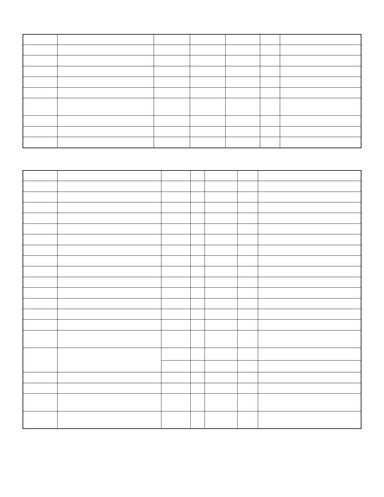
Negative High Voltage Output
Symbol
VNgate
RsourceN
RsinkN
triseN
tfallN
tpwn(min)
tdelayN
VNsen
tshortN
Parameter
Output voltage swing
VNgate source resistance
VNgate sink resistance
VNgate rise time
VNgate fall time
VNgate minimum pulse width
(internally limited)
NIN to VNgate delay time
VNgate current sense voltage
VNgate current sense OFF time
Control Circuitry
Symbol
Parameter
VIL
Logic input low voltage
VIH
Logic input high voltage
IINdn
Input pull-down current
Rup
Input pull-up resistance
VOL
Logic output low voltage
VOH
Logic output high voltage
VRST(OFF) Reset voltage, device off
VRST(ON) Reset voltage, device on
VRST(HYS) Reset hysteresis voltage
Ireset
Reset pull-up current
tRST(ON)
RESET on delay
tRST(OFF)
RESET off delay
tEN(ON)
ENABLE on delay
tEN(OFF)
ENABLE off delay
tFLT(HOLD) FAULT hold time
tDB
Deadband time
tdelay(N-P)
tdelay(P-N)
∆tdelay(N-P)
∆tdelay(P-N)
N-off to P-on transistion delay
P-off to N-on transistion delay
Delay difference
t - t delayN(off) delayP(on)
Delay difference
t - t delayP(off) delayN(on)
HV430
Min
Typ
Max
Unit
Conditions
VNN2
VNN1
V
No load on VNgate
15.0
Ω
IOUT=80mA
15.0
Ω IOUT=-80mA
50
ns Cload=1.0nF
50
ns Cload=1.0nF
100
VNN1+0.85
150
VNN1+1.0
200
ns
300
ns
VNN1+1.15 V
150
ns
mode=1
Min Typ
0
2.7
0.5
1
100 200
4.50
3.2
3.7
0.3
7
10
50 100
4
35
50
105 140
-80
0
Max
0.60
5.0
5
300
0.50
3.5
4.0
13
1.0
1.0
150
1.0
70
175
300
300
80
Unit
Conditions
V VDD=5.0V
V VDD=5.0V
µA PIN, NIN, ENABLE
kΩ MODE
V VDD=5.0V, IOUT=-0.5mA
V VDD=5.0V, IOUT=0.5mA
V VDD=5.0V
V VDD=5.0V
V VDD=5.0V
µA VRESET=0-4.5V
µs
µs
µs
µs
NIN/PIN
cycles
ENABLE=1
ns Mode=0, Rdb=5.6kΩ
ns Mode=0, Rdb=18kΩ
ns Mode=0, Rdb<27kΩ
ns Mode=0, Rdb<27kΩ
ns Mode=1
-80
0
80
ns Mode=1
3
Share Link: 