CY7C197-12PC(1995) データシートの表示(PDF) - Cypress Semiconductor
部品番号
コンポーネント説明
メーカー
CY7C197-12PC Datasheet PDF : 10 Pages
| |||
CY7C197
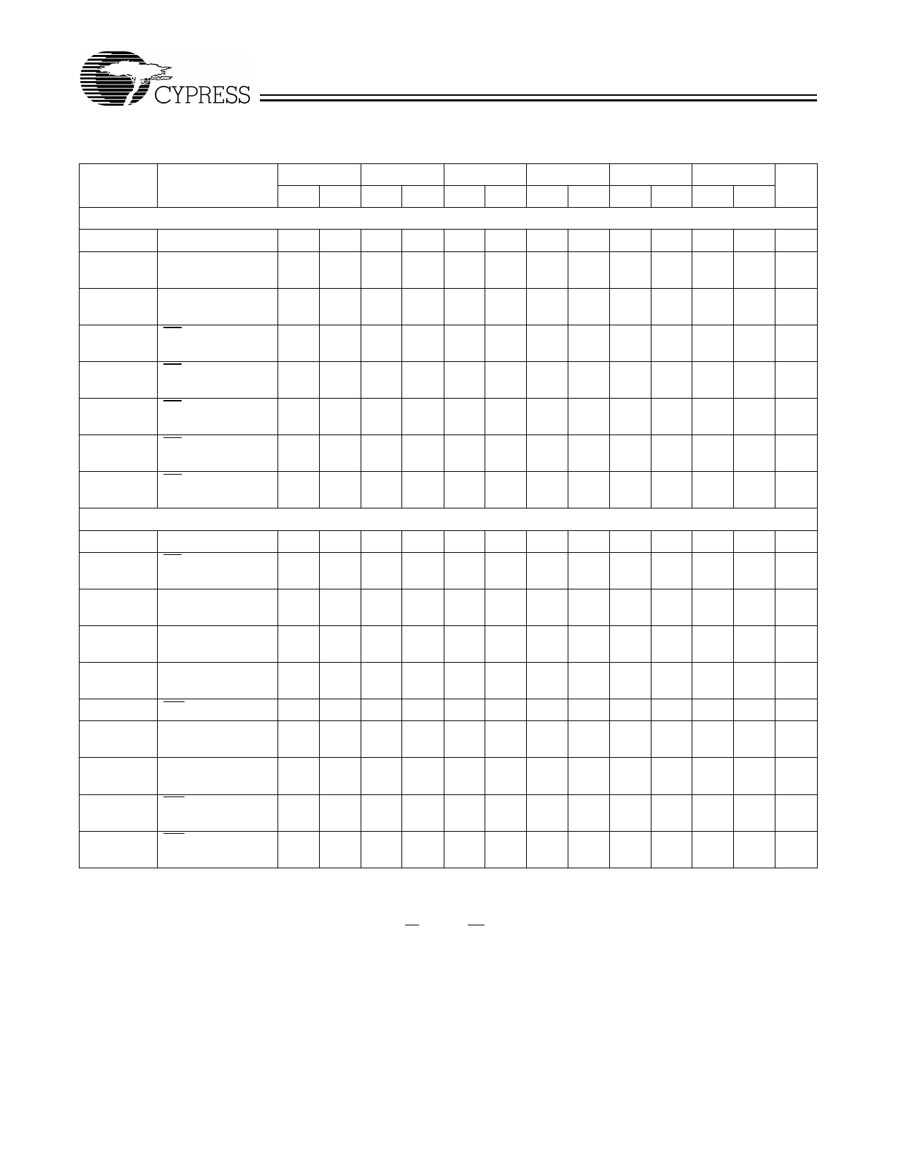
Switching Characteristics Over the Operating Range[3,8]
7C197-12 7C197-15 7C197-20 7C197-25 7C197-35 7C197-45
Parameter Description Min. Max. Min. Max. Min. Max. Min. Max. Min. Max. Min. Max. Unit
READ CYCLE
tRC
Read Cycle Time 12
15
20
25
35
45
ns
tAA
Address to
Data Valid
12
15
20
25
35
45 ns
tOHA
Output Hold from 3
3
3
3
3
3
ns
Address Change
tACE
CE LOW to
Data Valid
12
15
20
25
35
45 ns
tLZCE
CE LOW to
Low Z[9]
3
3
3
3
3
3
ns
tHZCE
CE HIGH to
High Z[9, 10]
5
7
0
9
0 11 0 15 0 15 ns
tPU
CE LOW to
0
0
0
0
0
0
ns
Power-Up
tPD
CE HIGH to
Power-Down
WRITE CYCLE[11]
12
15
20
20
25
30 ns
tWC
Write Cycle Time 12
15
20
25
35
45
ns
tSCE
CE LOW to
9
Write End
10
15
20
30
40
ns
tAW
Address Set-Up to 9
Write End
10
15
20
30
40
ns
tHA
Address Hold from 0
0
0
0
0
0
ns
Write End
tSA
Address Set-Up to 0
0
0
0
0
0
ns
Write Start
tPWE
tSD
WE Pulse Width
8
Data Set-Up to
8
Write End
9
15
20
25
30
ns
9
10
15
17
20
ns
tHD
Data Hold from
0
0
0
0
0
0
ns
Write End
tLZWE
WE HIGH to
Low Z[9]
2
2
3
3
3
3
ns
tHZWE
WE LOW to
High Z[9,10]
7
7
0 10 0 11 0 15 0 15 ns
Shaded area contains preliminary information.
Notes:
8. Test conditions assume signal transition time of 3 ns or less for −12 and −15 speeds and 5 ns or less for −20 and slower speeds, timing reference levels of
1.5V, input pulse levels of 0 to 3.0V, and output loading of the specified IOL/IOH and 30-pF load capacitance.
9.
10.
At any given temperature and voltage condition,
tHZCE and tHZWE are specified with CL = 5 pF as
tHZCE is less
in part (b) in
than tLZCE and
AC Test Loads
atHnZdWWE aisvelefossrmthsa. nTrtaLnZsWitEiofnorisanmyegaisvuernedde±v5ic0e0.
mV
from
steady-state
voltage.
11. The internal write time of the memory is defined by the overlap of CE LOW and WE LOW. Both signals must be LOW to initiate a write and either signal can
terminate a write by going HIGH. The data input set-up and hold timing should be referenced to the rising edge of the signal that terminates the write.
4
Share Link: 