CY7C197BN(2011) гғҮгғјгӮҝгӮ·гғјгғҲгҒ®иЎЁзӨәпјҲPDFпјү - Cypress Semiconductor
йғЁе“Ғз•ӘеҸ·
гӮігғігғқгғјгғҚгғігғҲиӘ¬жҳҺ
гғЎгғјгӮ«гғј
CY7C197BN Datasheet PDF : 13 Pages
| |||
AC Electrical Characteristics[4, 6, 7, 8]
Parameter
Description
tRC
tAA
tOHA
tACE
tLZCE
tHZCE
tPU
tPD
tWC
tSCE
tAW
tHA
tSA
tPWE
tSD
tHD
tHZWE
tLZWE
Read Cycle Time
Address to Data Valid
Data Hold from Address Change
CE to Data Valid
CE to Low Z
CE to High Z
CE to Power-up
CE to Power-down
Write Cycle Time
CE to Write End
Address Set-up to Write End
Address Hold from Write End
Address Set-up to Write Start
WE Pulse Width
Data Set-Up to Write End
Data Hold from Write End
WE LOW to High Z
WE HIGH to Low Z
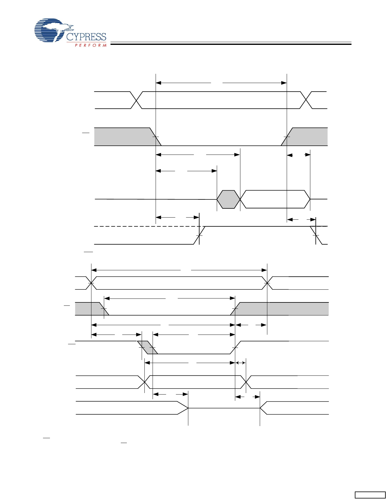
Timing Waveforms
Read Cycle No. 1 [9, 10]
Address
Data Out
tAA
tOHA
Previous Data Valid
CY7C197BN
15 ns
Min
Max
15
вҖ“
вҖ“
15
3
вҖ“
вҖ“
15
3
вҖ“
вҖ“
5
0
вҖ“
вҖ“
15
15
вҖ“
9
вҖ“
10
вҖ“
0
вҖ“
0
вҖ“
9
вҖ“
9
вҖ“
0
вҖ“
вҖ“
7
2
вҖ“
25 ns
Unit
Min
Max
25
вҖ“
ns
вҖ“
25
ns
3
вҖ“
ns
вҖ“
25
ns
3
вҖ“
ns
вҖ“
11
ns
0
вҖ“
ns
вҖ“
20
ns
25
вҖ“
ns
20
вҖ“
ns
20
вҖ“
ns
0
вҖ“
ns
0
вҖ“
ns
20
вҖ“
ns
15
вҖ“
ns
0
вҖ“
ns
вҖ“
11
ns
3
вҖ“
ns
tRC
Data Valid
Notes
6. At any given temperature and voltage condition, tHZCE is less than tLZCE, and tHZWE is less than tLZWE for any given device.
7. The internal Write time of the memory is defined by the overlap of CE LOW and WE LOW. CE and WE must be LOW to initiate a write, and the transition of any of
these signals can terminate the Write. The input data setup and hold timing should be referenced to the leading edge of the signal that terminates the write.
8. tHZCE, tHZWE are specified as in part (b) of the AC Test Loads[5] on page 5. Transitions are measured Вұ200 mV from steady state voltage.
9. Device is continuously selected. CE = VIL.
10. WE is HIGH for Read Cycle.
Document #: 001-06447 Rev. *C
Page 6 of 13
[+] Feedback
Share Link: 