CY7C4201-15AXC データシートの表示(PDF) - Cypress Semiconductor
部品番号
コンポーネント説明
メーカー
CY7C4201-15AXC Datasheet PDF : 19 Pages
| |||
CY7C4421/4201/4211/4221
CY7C4231/4241/4251
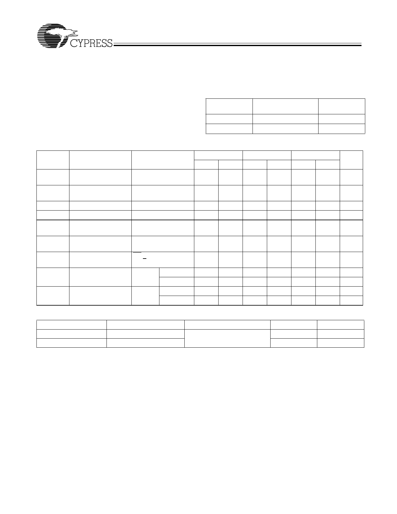
Maximum Ratings[4]
(Above which the useful life may be impaired. For user guide-
lines, not tested.)
Storage Temperature ...................................–65°C to +150°C
Ambient Temperature with
Power Applied...............................................–55°C to +125°C
Supply Voltage to Ground Potential ............... –0.5V to +7.0V
DC Voltage Applied to Outputs
in High-Z State ............................................... –0.5V to +7.0V
DC Input Voltage............................................ –3.0V to +7.0V
Electrical Characteristics Over the Operating Range[6]
Output Current into Outputs (LOW)............................. 20 mA
Static Discharge Voltage........................................... > 2001V
(per MIL-STD-883, Method 3015)
Latch-up Current..................................................... > 200 mA
Operating Range
Range
Commercial
Industrial[5]
Ambient
Temperature
0°C to +70°C
–40°C to +85°C
VCC
5V ±10%
5V ±10%
-10
-15
-25
Parameter
Description
Test Conditions
Min. Max. Min. Max. Min. Max. Unit
VOH
VOL
VIH
VIL
IIX
IOS[7]
IOZL
IOZH
ICC1[8]
ICC2[9]
Output HIGH Voltage
Output LOW Voltage
Input HIGH Voltage
Input LOW Voltage
VCC = Min.,
IOH = –2.0 mA
VCC = Min.,
IOL = 8.0 mA
2.4
2.4
2.4
V
0.4
0.4
0.4
V
2.2
VCC
2.2
VCC
2.2
VCC
V
–3.0 0.8 –3.0 0.8 –3.0 0.8
V
Input Leakage
Current
VCC = Max.
–10
+10
–10
+10
–10
+10
µA
Output Short
VCC = Max.,
–90
–90
–90
mA
Circuit Current
VOUT = GND
Output OFF,
High-Z Current
OE > VIH,
VSS < VO < VCC
–10 +10 –10 +10 –10 +10 mA
Active Power Supply
Commercial
35
35
35
mA
Current
Industrial
40
40
40
mA
Average Standby
Current
Commercial
10
10
10
mA
Industrial
15
15
15
mA
Capacitance[10]
Parameter
Description
Test Conditions
CIN
COUT
Input Capacitance
Output Capacitance
TA = 25°C, f = 1 MHz,
VCC = 5.0V
Notes:
4. The Voltage on any input or I/O pin cannot exceed the power pin during power-up.
5. TA is the “instant on” case temperature.
6. See the last page of this specification for Group A subgroup testing information.
7. Test no more than one output at a time for not more than one second.
8. Outputs open. Tested at Frequency = 20 MHz.
9. All inputs = VCC – 0.2V, except WCLK and RCLK, which are switching at 20 MHz.
10. Tested initially and after any design or process changes that may affect these parameters.
Max.
Unit
5
pF
7
pF
Document #: 38-06016 Rev. *C
Page 7 of 19
Share Link: 