STK1744-D35I データシートの表示(PDF) - Simtek Corporation
部品番号
コンポーネント説明
メーカー
STK1744-D35I Datasheet PDF : 12 Pages
| |||
STK1744
ABSOLUTE MAXIMUM RATINGSa
Voltage on Input Relative to Ground . . . . . . . . . . . . . .–0.5V to 7.0V
Voltage on Input Relative to VSS . . . . . . . . . . –0.6V to (VCC + 0.5V)
Voltage on DQ0-7. . . . . . . . . . . . . . . . . . . . . . –0.5V to (VCC + 0.5V)
Temperature under Bias . . . . . . . . . . . . . . . . . . . . . . –55°C to 85°C
Storage Temperature . . . . . . . . . . . . . . . . . . . . . . . . –65°C to 85°C
Power Dissipation . . . . . . . . . . . . . . . . . . . . . . . . . . . . . . . . . . . . 1W
DC Output Current (1 output at a time, 1s duration) . . . . . . . . 15mA
Note a:
Stresses greater than those listed under “Absolute Maximum Rat-
ings” may cause permanent damage to the device. This is a stress
rating only, and functional operation of the device at conditions
above those indicated in the operational sections of this specifica-
tion is not implied. Exposure to absolute maximum rating condi-
tions for extended periods may affect reliability.
DC CHARACTERISTICS
(VCC = 5.0V ± 10%)
SYMBOL
ICC1b
PARAMETER
Average VCC Current
ICC2
ICC3b
ISB1c
ISB2c
IILK
IOLK
VIH
VIL
VOH
VOL
TA
Average VCC Current during STORE
5AVv,e2ra5g°eC,VTCyCpiCcaulrrent at tAVAV = 200ns
Average VCC Current
(Standby, Cycling TTL Input Levels)
VCC Standby Current
(Standby, Stable CMOS Input Levels)
Input Leakage Current
Off-State Output Leakage Current
Input Logic “1” Voltage
Input Logic “0” Voltage
Output Logic “1” Voltage
Output Logic “0” Voltage
Operating Temperature
COMMERCIAL
MIN
MAX
97
80
70
3
10
30
25
22
1.5
INDUSTRIAL
MIN
MAX
100
85
70
3
10
31
26
23
1.5
UNITS
mA
mA
mA
mA
mA
mA
mA
mA
mA
±1
±1
µA
±5
±5
µA
2.2
VCC + .5
2.2 VCC + .5
V
VSS – .5
0.8 VSS – .5 0.8
V
2.4
2.4
V
0.4
0.4
V
0
70
– 40
85
°C
NOTES
tAVAV = 25ns
tAVAV = 35ns
tAVAV = 45ns
All Inputs Don’t Care, VCC = max
W ≥ (V CC – 0.2V)
All Others Cycling, CMOS Levels
tAVAV = 25ns, E ≥ VIH
tAVAV = 35ns, E ≥ VIH
tAVAV = 45ns, E ≥ VIH
E ≥ (V CC – 0.2V)
All Others VIN ≤ 0.2V or ≥ (VCC – 0.2V)
VCC = max
VIN = VSS to VCC
VCC = max
VIN = VSS to VCC, E or G ≥ VIH
All Inputs
All Inputs
IOUT = – 4mA
IOUT = 8mA
Note b:
Note c:
IECC≥1VaIHndwIiCll Cn3otapreroddeupceensdteanntdobny
output loading and
current levels until
cycle rate. The
any nonvolatile
specified values are obtained at
cycle in progress has timed out.
minimum
cycle
with
outputs
unloaded.
AC TEST CONDITIONS
Input Pulse Levels . . . . . . . . . . . . . . . . . . . . . . . . . . . . . . . 0V to 3V
Input Rise and Fall Times . . . . . . . . . . . . . . . . . . . . . . . . . . . . . . . ≤ 5ns
Input and Output Timing Reference Levels . . . . . . . . . . . . . . . 1.5V
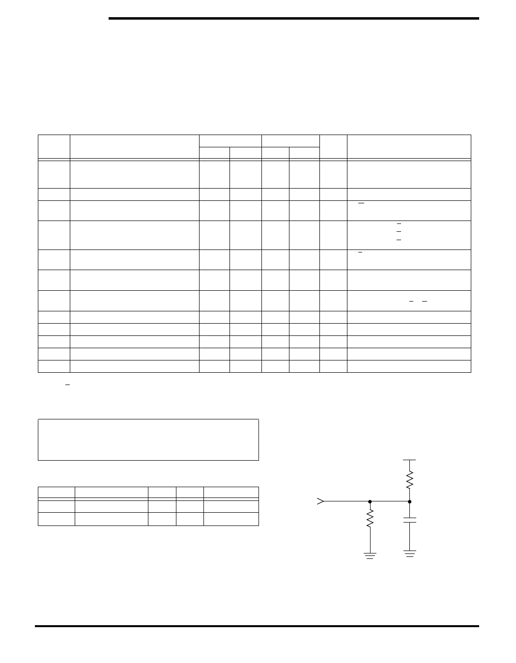
Output Load . . . . . . . . . . . . . . . . . . . . . . . . . . . . . . . . . See Figure 1
5.0V
CAPACITANCEd (TA = 25°C, f = 1.0MHz)
SYMBOL
CIN
COUT
PARAMETER
Input Capacitance
Output Capacitance
MAX
10
12
UNITS
pF
pF
CONDITIONS
∆V = 0 to 3V
∆V = 0 to 3V
Note d: These parameters are guaranteed but not tested.
OUTPUT
255 Ohms
480 Ohms
30 pF
INCLUDING
SCOPE AND
FIXTURE
Figure 1: AC Output Loading
January 2003
2 Document Control # ML0020 rev 0.0
Share Link: 