NX29F010-45PLI データシートの表示(PDF) - NexFlash -> Winbond Electronics
部品番号
コンポーネント説明
メーカー
NX29F010-45PLI
NexFlash -> Winbond Electronics

NX29F010-45PLI Datasheet PDF : 25 Pages
| |||
NX29F010
WRITE OPERATION STATUS
The device provides several bits to determine the status of
a write operation: DQ3, DQ5, DQ6, and DQ7. DQ7 and DQ6
each offer a method for determining whether a program or
erase operation is complete or in progress. Table 6 and the
following subsections describe the functions of these bits.
DQ7: Data Polling
The Data Polling bit, DQ7, indicates to the host system
whether an Embedded Algorithm is in progress or com-
pleted. Data Polling is valid after the rising edge of the final
WE pulse in the program or erase command sequence.
During the Embedded Program algorithm, the device
outputs on DQ7 the complement of the datum programmed
to DQ7. When the Embedded Program algorithm is com-
plete, the device outputs the true datum programmed to
DQ7. The system must provide the program address to read
valid status information on DQ7. If a program address falls
within a protected sector, Data Polling on DQ7 is active for
approximately 2 µs, then the device returns to reading array
data.
During the Embedded Erase algorithm, Data Polling pro-
duces a "0" on DQ7. When the Embedded Erase algorithm
is complete, Data Polling produces a "1" on DQ7. This is
analogous to the complement/true datum output described
for the Embedded Program algorithm: the erase function
changes all the bits in a sector to "1"; prior to this, the device
outputs the "complement," or "0". The system must provide
an address within any of the sectors selected for erasure to
read valid status information on DQ7.
After an erase command sequence is written, if all sectors
selected for erasing are protected, Data Polling on DQ7 is
active for approximately 100 µs, then the device returns to
reading array data. If not all selected sectors are protected,
the Embedded Erase algorithm erases the unprotected
sectors, and ignores the selected sectors that are
protected.
When the system detects DQ7 has changed from the
complement to true data, it can read valid data at DQ7-DQ0
on the following read cycles. This is because DQ7 may
change asynchronously with DQ0-DQ6 while Output Enable
(OE) is asserted low. The Data Polling Timings (During
Embedded Algorithms) figure in the "AC Characteristics"
section illustrates this.
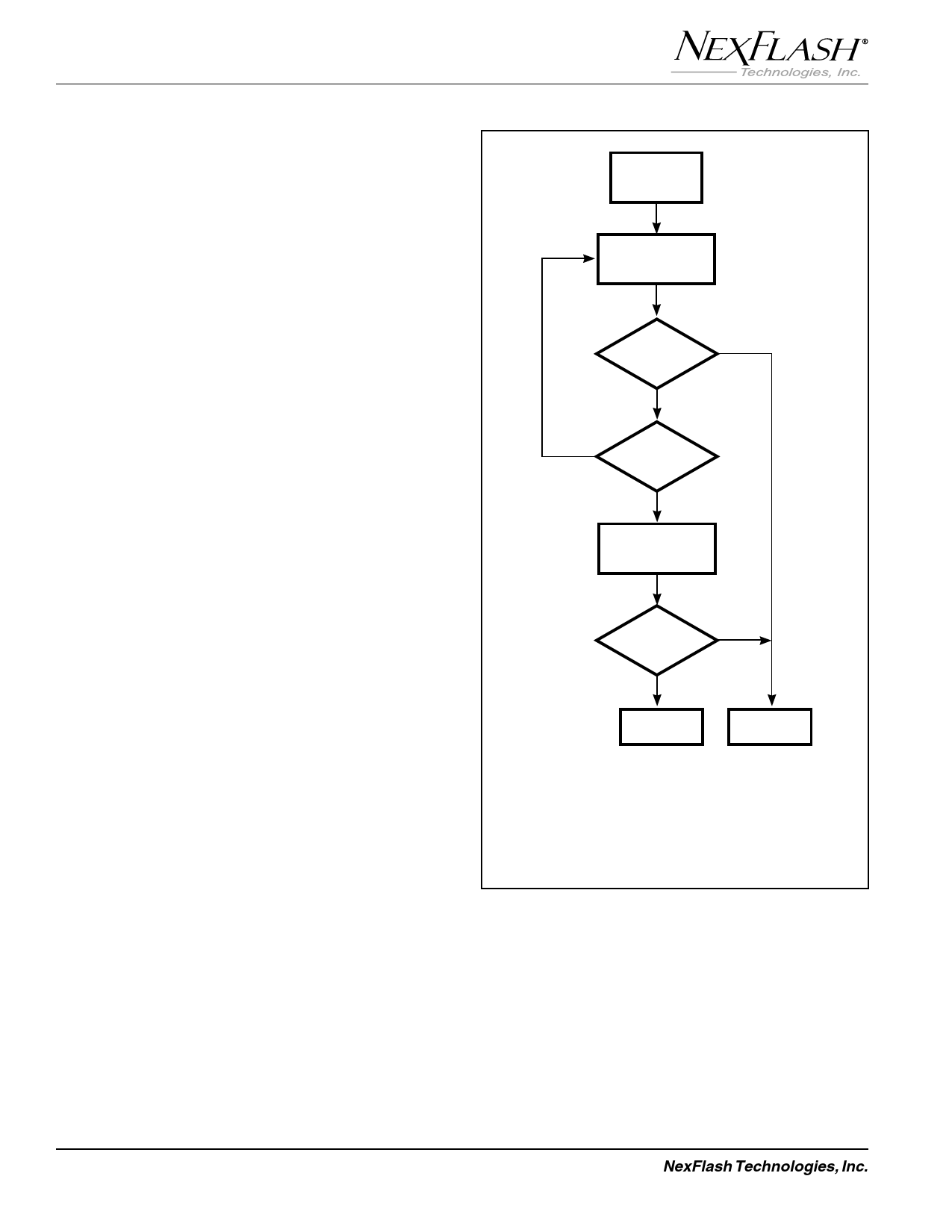
START
READ
DQ7-DQ0
ADDR = VA
DQ7 = DATA?
YES
NO
NO
DQ5 = 1?
YES
READ
DQ7-DQ0
ADDR = VA
DQ7 = DATA?
YES
NO
FAIL
PASS
Notes:
1. VA = Valid address for programming. During a sector
erase operation, a valid address is an address within
any sector selected for erasure. During chip erase, a
valid address is any non-protected sector address.
2. DQ7 should be rechecked even if DQ5 ="1" because
DQ7 may change simultaneously with DQ5.
Figure 7. Data Polling Algorithm
Table 6 shows the outputs for Data Polling on DQ7.
Figure 7 shows the Data Polling algorithm.
10
NexFlash Technologies, Inc.
NXPF001F-0600
06/22/00 ©
Share Link: