NX29F010-35W データシートの表示(PDF) - NexFlash -> Winbond Electronics
部品番号
コンポーネント説明
メーカー
NX29F010-35W
NexFlash -> Winbond Electronics

NX29F010-35W Datasheet PDF : 25 Pages
| |||
NX29F010
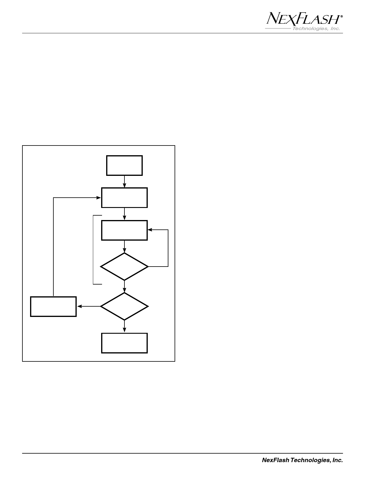
Commands written to the device while the Embedded
Program Algorithm is in progress are ignored.
Programming is allowed in any sequence and across sector
boundaries. A bit cannot be programmed from a '0' back
to a '1'. Attempting to do so may halt the operation and set
the error status bit, DQ5, to '1', or cause the Data Polling
algorithm to indicate the operation was successful.
However, a succeeding read will show that the data is still
'0'. Only erase operations can convert a '0' to a '1'.
Note: See Command Definitions (Table 5) for program
command sequence.
START
WRITE PROGRAM
COMMAND
SEQUENCE
EMBEDDED
PROGRAM
ALGORITHM
IN PROGRESS
DATA POLL
FROM
SYSTEM
VERIFY
NO
DATA?
YES
INCREMENT
ADDRESS
NO
LAST
ADDRESS?
YES
PROGRAMMING
COMPLETE
Figure 5. Program Operation
Chip Erase Command Sequence
Chip erase is a six-bus-cycle operation. The chip erase
command sequence is initiated by writing two unlock
cycles, followed by a setup command. Two additional
unlock write cycles are then followed by the chip erase
command, which in turn invokes the Embedded Erase
algorithm. The device does not require the system to
preprogram prior to erase. The Embedded Erase algorithm
automatically preprograms and verifies the entire memory
for an all zero data pattern prior to electrical erase. The
system is not required to provide any controls or timings
during these operations. The Command Definitions table
shows the address and data requirements for the chip erase
command sequence.
Commands written to the chip while the Embedded Erase
Algorithm is in progress are ignored.
The system can determine the status of the erase operation
by using DQ7 or DQ6. See "Write Operation Status" for
information on these status bits. When the Embedded
Erase algorithm is complete, the device returns to reading
array data and addresses are no longer latched.
Figure 6 illustrates the algorithm for the erase operation.
See the Erase/Program Operations tables in "AC Charac-
teristics" for parameters, and to the Chip/Sector Erase
Operation Timings for timing waveforms.
Sector Erase Command Sequence
Sector erase is a six bus cycle operation. The sector erase
command sequence is initiated by writing two unlock cycles,
followed by a setup command. Two additional unlock write
cycles are then followed by the address of the sector to be
erased, and the sector erase command. The Command
Definitions Table (Table 5) shows the address and data
requirements for the sector erase command sequence.
The device does not require the system to preprogram the
memory prior to erase. The embedded erase algorithm
automatically programs and verifies the sector for an all
zero data pattern prior to electrical erase. The system is not
required to provide any controls or timings during these
operations.
8
NexFlash Technologies, Inc.
NXPF001F-0600
06/22/00 ©
Share Link: