HV301LG データシートの表示(PDF) - Supertex Inc
部品番号
コンポーネント説明
メーカー
HV301LG Datasheet PDF : 21 Pages
| |||
Functional Description, cont’d.
RAMP pin will be fixed, indicating that the circuit is in current limit
mode. Depending on the value of the load capacitor and the
programmed current limit, charging may continue for some time,
but may not exceed a nominal 100ms preset time limit. Once the
load capacitor has been charged, the output current will drop,
reducing the voltage on the SENSE pin, which in turn will
increase the RAMP pin current, thus causing the voltage on the
capacitor connected to the RAMP pin to continue rising, thereby
providing yet another programmed delay. If due to output over-
load conditions during startup, PWRGD does not achieve an
active state within 100ms or the circuit breaker is tripped, the
circuit is reset, pulling down the GATE to VEE, discharging the
capacitor connected to the RAMP pin, changing PWRGD to an
inactive state. A timeout or circuit breaker fault will initiate an
auto-retry if enabled.
On the other hand, in feedback capacitor mode, a current source
of 10µA from the RAMP pin limits the dv/dt of the feedback
capacitor which, in turn, programs Inrush according to
HV301/HV311
Inrush ~ 10µA•Cload/C2. (See Programming Inrush and ICB for
accurate formula on page 6.)
When the ramp voltage is within 1.2V of the regulated internal
supply voltage, the controller will force the GATE terminal to a
nominal 10V, the PWRGD pin will change to an active state, the
circuit breaker supervisor is enabled and the circuit will transition
to a low power sleep mode.
When the voltage on the SENSE pin rises to 100mV, indicating
an over current condition, the circuit breaker will trip in less than
5µs. This time may be extended by the addition of external
components.
At any time during the start up cycle or thereafter, crossing the
UV and OV limits (including hysteresis) will cause an immediate
reset of all internal circuitry. When the input supply voltage
returns to a value within the programmed UV and OV limits a new
start up sequence will be initiated.
Design Information
Setting UnderVoltage and OverVoltage Shut Down
The UV and OV pins are connected to comparators with nominal
1.21V thresholds and 100mV of hysteresis (1.21V ± 50mV).
They are used to detect under voltage and over voltage condi-
tions at the input to the circuit. Whenever the OV pin rises above
its high threshold (1.26V) or the UV pin falls below its low
threshold (1.16V) the GATE voltage is immediately pulled low,
the PWRGD pin changes to its inactive state and the external
capacitor connected to the RAMP pin is discharged.
Calculations can be based on either the desired input voltage
operating limits or the input voltage shutdown limits. In the
following equations the shutdown limits are assumed.
The undervoltage and overvoltage shut down thresholds can be
programmed by means of the three resistor divider formed by
R1, R2 and R3. Since the input currents on the UV and OV pins
are negligible the resistor values may be calculated as follows:
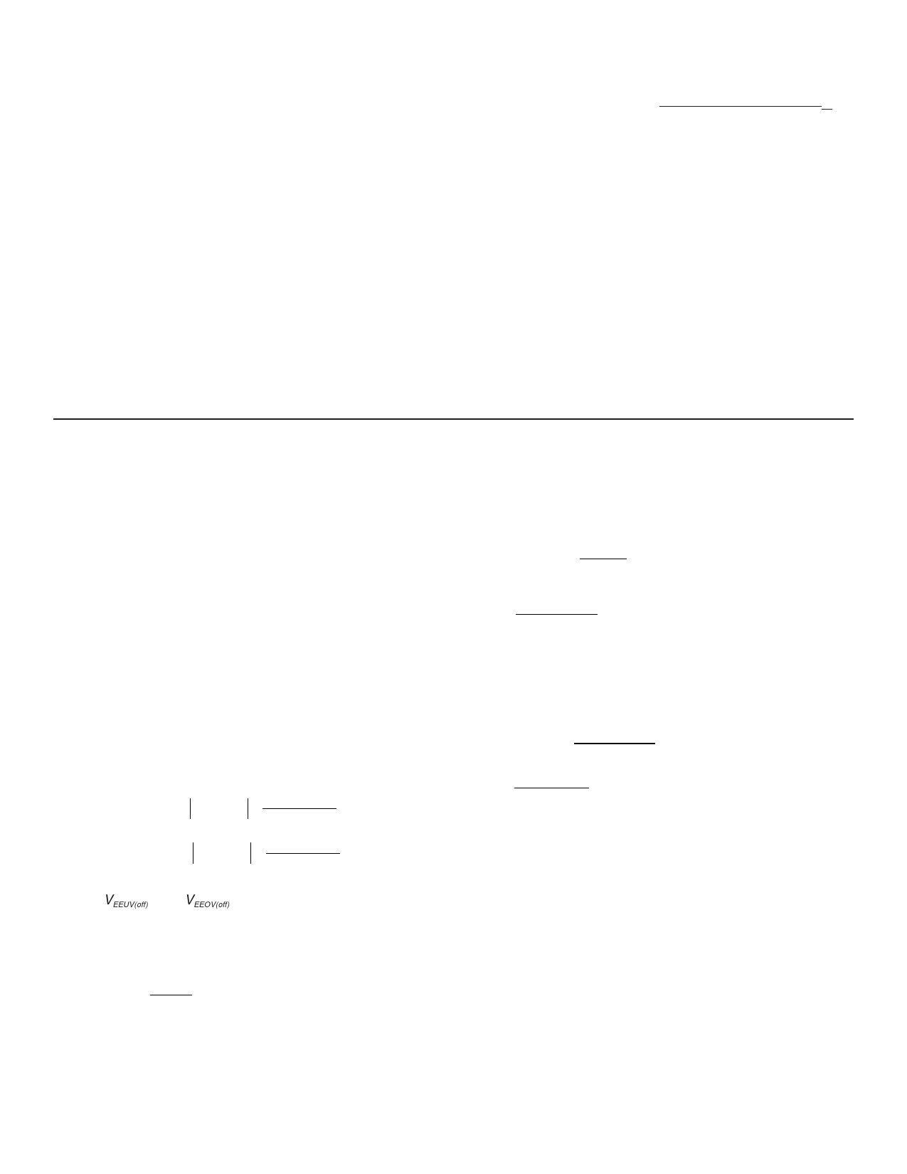
UVOFF
=
VUVL
= 1.16
=
VEEUV(off )
×
R2 + R3
R1 + R2 + R3
OVOFF
= VOVH
= 1.26
=
VEEOV(off )
×
R1 +
R3
R2 +
R3
Where |VEEUV(off)| and |VEEOV(off)| relative to VEE are Under & Over
Voltage Shut Down Threshold points.
If we select a divider current of 100µA at a nominal operating
input voltage of 50 Volts then
R1 + R2 + R3 = 50V = 500kΩ
100µA
From the second equation for an OV shut down threshold of 65V
the value of R3 may be calculated.
OVOFF
= 1.26
=
65 × R3
500kΩ
R3 = 1.26 × 500kΩ = 9.69kΩ
65
The closest 1% value is 9.76kΩ.
From the first equation for a UV shut down threshold of 35V the
value of R2 can be calculated.
UVOFF
=
1.16
=
35 × (R2 + R3)
500kΩ
R2 = 1.16 × 500kΩ − 9.76kΩ = 6.81kΩ
35
The closest 1% value is 6.81kΩ.
Then
R1 = 500kΩ − R2 − R3 = 483kΩ
The closest 1% value is 487kΩ.
5
Share Link: 