HT19 データシートの表示(PDF) - Supertex Inc
部品番号
コンポーネント説明
メーカー
HT19 Datasheet PDF : 4 Pages
| |||
Logic Truth Table
HKS
H
H
L or Z
L or Z
X
Z = high impedance, open circuit
X = irrelevant
L = logic level low
H = logic level high
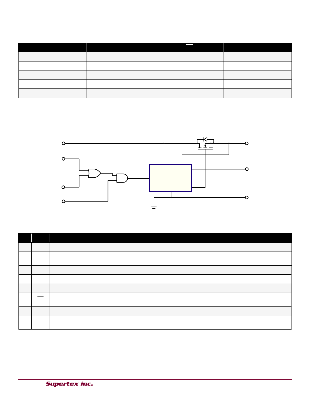
Block Diagram
(1)
TPG
(2)
HKS
(5)
LS
(6)
DP
LS
L or Z
H
L or Z
H
X
DP
H or Z
H or Z
H or Z
H or Z
L
H = ON
L = OFF
Charge Pump
and
Logic Control
HT19
Switch State
ON
ON
OFF
ON
OFF
(8)
TP
(7)
CS
(3)
GND
Pin Description
Pin Name Description
1 TPG Positive input side of a telephone line, typically tip side.
2
HKS
Hookswitch input. Connect HKS to TPG to turn on the hook switch. Internally pulled low with a high value
resistor.
3 GND Device ground. Negative side of a telephone line, typically ring side.
4 NC No connect. Open circuit. No internal connections to the device.
5 LS Line switch input. Input logic high turns on the hook switch. Internally pulled low with a high value resistor.
6
DP
Dial pulse input. Input logic low turns off the hook switch. Used for pulse dialing. Internally pulled high with
a high value resistor.
7 CS Current sense input. An external resistor connected between CS and TP sets the current limit.
8
TP
Positive output side of a telephone line. Zener protection to prevent this output from rising above 18V is
required.
● 1235 Bordeaux Drive, Sunnyvale, CA 94089 ● Tel: 408-222-8888 ● www.supertex.com
3
Share Link: 