DG2735DN-T1-E4 データシートの表示(PDF) - Vishay Semiconductors
部品番号
コンポーネント説明
メーカー
DG2735DN-T1-E4 Datasheet PDF : 10 Pages
| |||
DG2735, DG2736
Vishay Siliconix
Low Voltage, 0.6 , Dual SPDT Analog Switch
DESCRIPTION
The DG2735, DG2736 are low voltage, low on-resistance,
dual single-pole/double-throw (SPDT) monolithic CMOS
analog switches designed for high performance switching of
analog signals. Combining low-power, high speed, low
on-resistance, and small package size, the DG2735,
DG2736 are ideal for portable and battery power
applications.
The DG2735, DG2736 have an operation range from 1.65 V
to 4.3 V single supply. The DG2735 has two separate control
pins with for the separated two SPDT switched. The DG2736
has an EN pin. All switches are at high impedance mode
when the EN is high.
The DG2735, DG2736 are guaranteed 1.65 V logic
compatible, allowing the easy interface with low voltage DSP
or MCU control logic and ideal for one cell Li-ion battery
direct power.
The switch conducts signals within power rails equally well in
both directions when on, and blocks up to the power supply
level when off. Break-before-make is guaranteed.
The DG2735, DG2736 are built on Vishay Siliconix’s sub
micron CMOS low voltage process technology and provides
greater than 300 mA latch-up protection, as tested per
JESD78.
As a committed partner to the community and the
environment, Vishay Siliconix manufactures this product with
lead (Pb)-free device terminations. DG2735, DG2736 are
offered in a miniQFN package. The miniQFN package has a
nickel-palladium-gold device termination and is represented
by the lead (Pb)-free “-E4” suffix. The nickel-palladium-gold
device terminations meet all JEDEC standards for reflow and
MSL ratings.
FEATURES
• Low voltage operation (1.65 V to 4.3 V)
• Low on-resistance - RON: 0.6 at 2.7 V
• Fast switching: tON = 55 ns at 2.7 V
• TOFF = 40 ns at 2.7 V
• Latch-up current > 300 mA (JESD78)
• Material categorization: For definitions of compliance
please see www.vishay.com/doc?99912
BENEFITS
• Reduced power consumption
• High accuracy
• Reduce board space
• TTL/1.65 V logic compatible
APPLICATIONS
• Cellular phones
• Speaker headset switching
• Audio and video signal routing
• PCMCIA cards
• Battery operated systems
• Portable media player Handheld test instruments
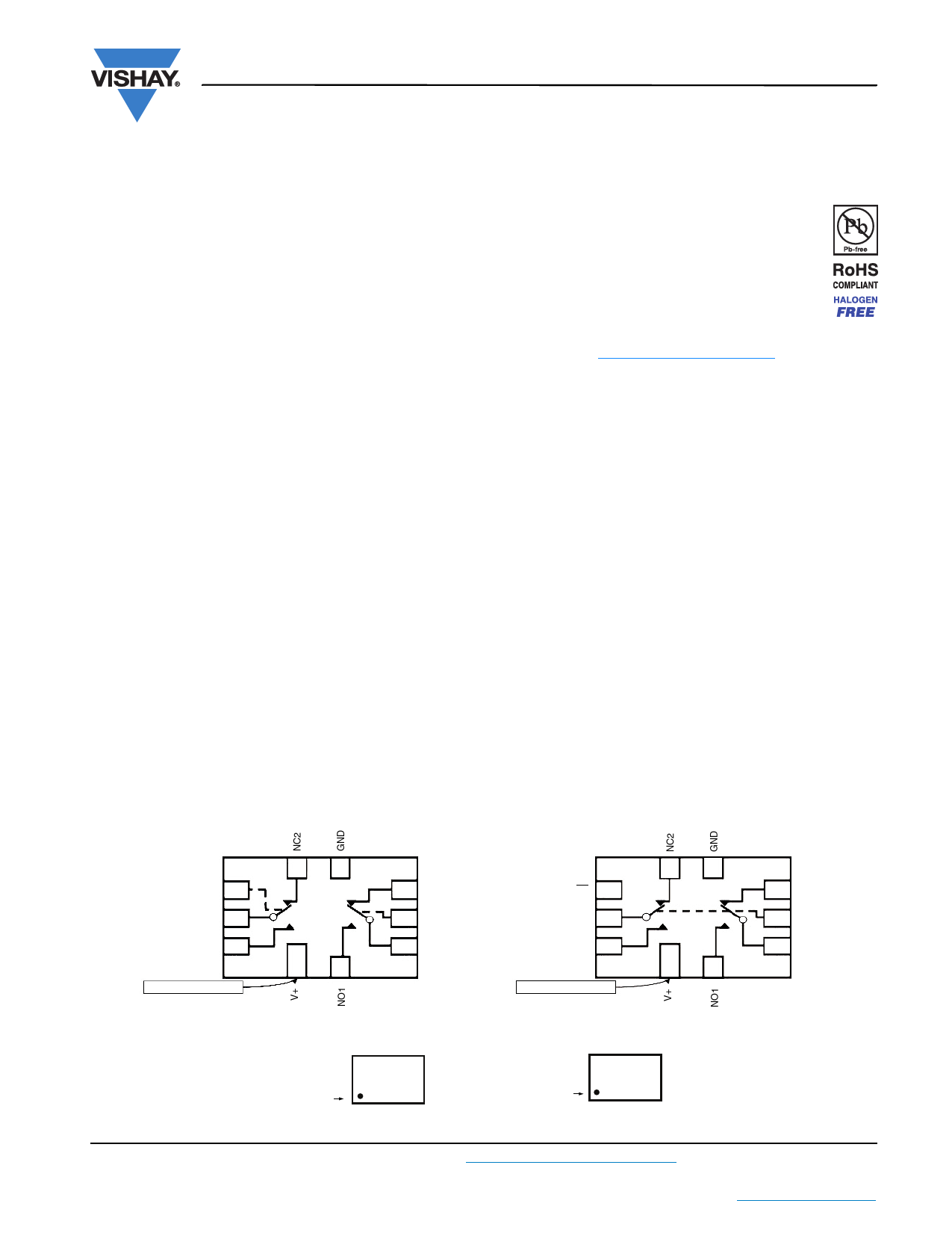
FUNCTIONAL BLOCK DIAGRAM AND PIN CONFIGURATION
DG2735
miniQFN-10L
DG2736
miniQFN-10L
IN2 8
COM2 9
NO2 10
Pin 1: LONG LEAD
7
6
5 NC1
EN 8
7
6
4 IN1
COM2 9
1
2
3 COM1
NO2 10
Pin 1: LONG LEAD
1
2
(Top View)
Device Marking: Ax for DG2735
Device Marking: Bx for DG2736
x = Date/Lot Traceability Code
(Top View)
Ax
Pin 1
or
Bx
Pin 1
5 NC1
4 IN1
3 COM1
Note: Pin 1 has long lead
Document Number: 74420
For technical questions, contact: analogswitchtechsupport@vishay.com
www.vishay.com
S12-2498-Rev. D, 22-Oct-12
1
This document is subject to change without notice.
THE PRODUCTS DESCRIBED HEREIN AND THIS DOCUMENT ARE SUBJECT TO SPECIFIC DISCLAIMERS, SET FORTH AT www.vishay.com/doc?91000
Share Link: 