DG2741DQ-T1(2003) データシートの表示(PDF) - Vishay Semiconductors
部品番号
コンポーネント説明
メーカー
DG2741DQ-T1 Datasheet PDF : 7 Pages
| |||
DG2741/2742/2743
Vishay Siliconix
New Product
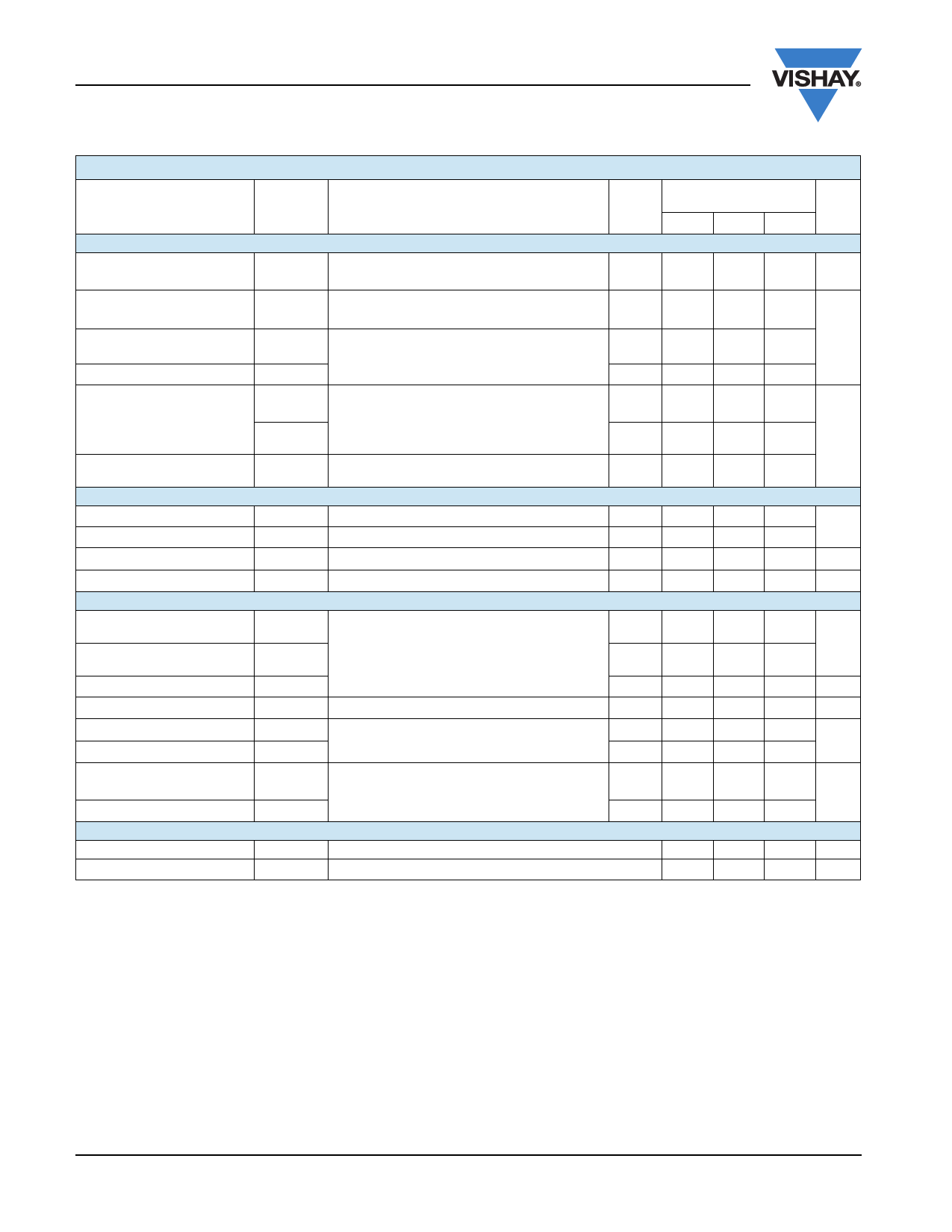
SPECIFICATIONS (V+ = 3.0 V)
Parameter
Analog Switch
Symbol
Test Conditions
Otherwise Unless Specified
V+ = 3 V, "10%, VIN = 0.5 or 1.4 Ve
Tempa
Limits
−40 to 85_C
Minb Typc Maxb
Analog Signal Ranged
On-Resistance
rON Flatness
rON MatchFlat
Switch Off Leakage Current
Channel-On Leakage Current
VNO, VNC,
VCOM
Full
0
rON
V+ = 2.7 V, VCOM = 0.2 V/1.5 V, INO
INC = 100 mA
Room
Full
rON
Flatness
DrON
V+ = 2.7 V, VCOM = 1.5, 2 V, INO, INC = 100 mA
Room
Room
INO(off),
INC(off)
ICOM(off)
V+ = 3.3 V
VNO, VNC = 0.3 V/3 V, VCOM = 3 V/0.3 V
Room
−1
Full
−10
Room
−1
Full
−10
ICOM(on)
V+ = 3.3 V, VNO, VNC = VCOM = 0.3 V/3 V
Room
−1
Full
−10
0.4
0.08
0.05
V+
0.8
0.9
0.18
0.08
1
10
1
10
1
10
Digital Control
Input High Voltage
Input Low Voltage
Input Capacitanced
Input Currentf
Dynamic Characteristics
VINH
VINL
Cin
IINL or IINH
VIN = 0 or V+
Full
1.4
Full
0.5
Full
5.5
Full
−1
1
Turn-On Time
Turn-Off Time
Break-Before-Make Time
Charge Injectiond
Off-Isolationd
Crosstalkd
NO, NC Off Capacitanced
Channel-On Capacitanced
Power Supply
tON
Room
Full
tOFF
VNO or VNC = 1.5 V, RL = 50 W, CL = 35 pF
V+ = 2.7 V, Figure 1 and 2
Room
Full
td
Room
1
QINJ
CL = 1 nF, VGEN = 0 V, RGEN = 0 W, Figure 3
Room
OIRR
XTALK
RL = 1 kW, CL = 5 pF, f = 1 MHz
Room
Room
CNO(off),
CNC(off)
CON
V+ = 3.6 V, VIN = 0 or V+, f = 1 MHz
Room
Room
20
30
35
18
28
33
5.8
−56
−89
81
103
Power Supply Range
V+
Power Supply Current
I+
V+ = 3.6 V, VIN = 0 or V+
1.5
3.6
0.01
1.0
Notes:
a. Room = 25°C, Full = as determined by the operating suffix.
b. The algebraic convention whereby the most negative value is a minimum and the most positive a maximum, is used in this data sheet.
c. Typical values are for design aid only, not guaranteed nor subject to production testing.
d. Guarantee by design, nor subjected to production test.
e. VIN = input voltage to perform proper function.
f. Guaranteed by 3-V leakage testing, not production tested.
Unit
V
W
nA
V
pF
mA
ns
pC
dB
pF
V
mA
www.vishay.com
4
Document Number: 72708
S-32617—Rev. A, 29-Dec-03
Share Link: 