DG449 データシートの表示(PDF) - Vishay Semiconductors
部品番号
コンポーネント説明
メーカー
DG449 Datasheet PDF : 10 Pages
| |||
DG449
Vishay Siliconix
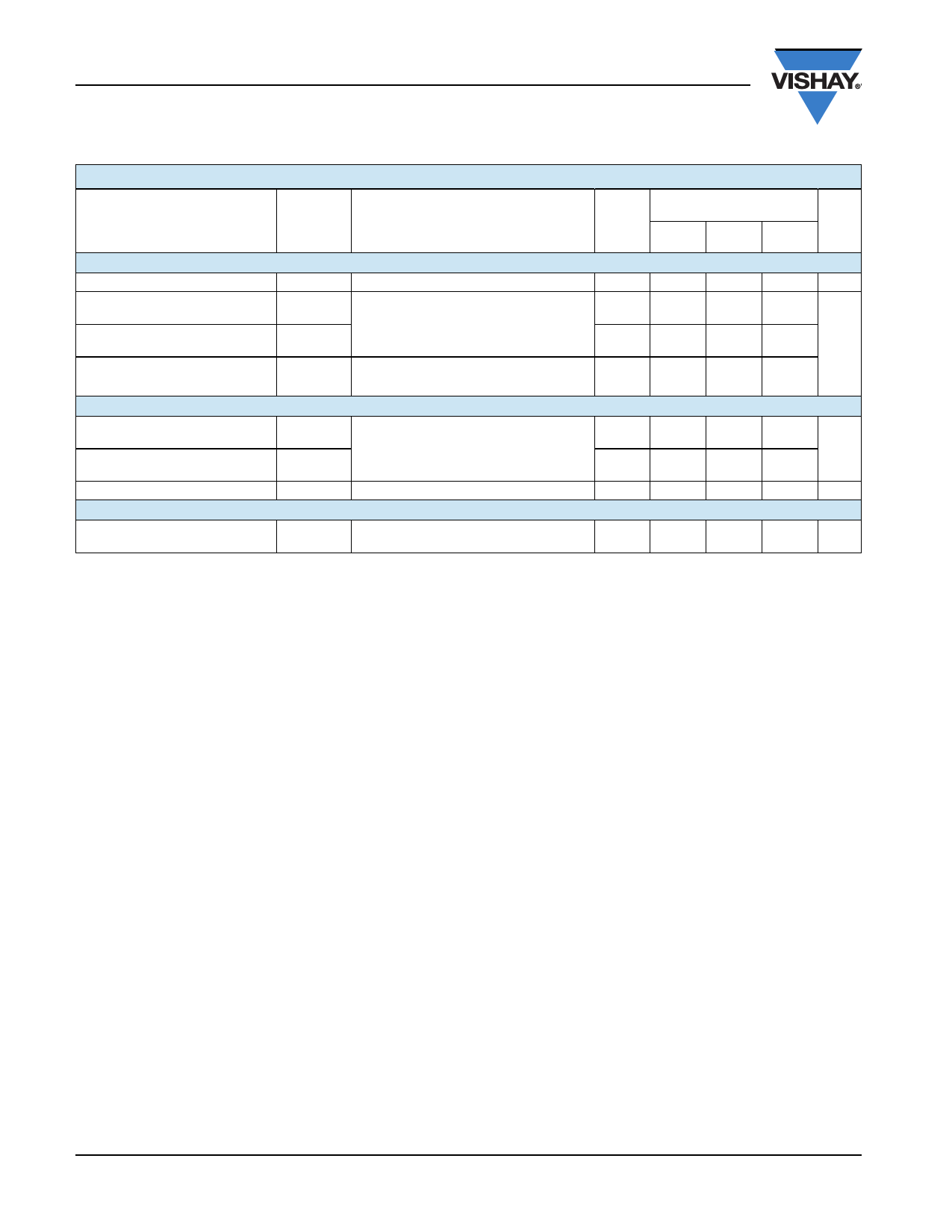
SPECIFICATIONSa
Parameter
Analog Switch
Analog Signal Rangee
On-Resistance
On-Resistance MATCH
On-Resistance Flatness
Symbol
VANALOG
RON
RON
RON
Flatness
Test Conditions
Unless Otherwise Specified
V+ = 12 V, V- = 0 V
VIN = 2.4 V, 0.8 Vf
Ino/nc = 1 mA, VCOM = 3, 8 V
V+ = 10.8 V
Ino/nc = 1 mA, VCOM = 2, 6, 10 V
V+ = 10.8 V
D Suffix
- 40 °C to 85 °C
Temp.b Min.d Typ.c Max.d Unit
Full
0
Room
Full
Room
Full
Room
Full
12
V
67
85
96
4
5
17
25
31
Dynamic Characteristics
Turn-On Time
Turn-Off Time
Charge Injectione
tON
Room
Full
tOFF
VNO, NC = 10 V, RL = 300 , CL = 35 pF
Room
Full
Q
CL = 1 nF, Vgen = 0 V, Rgen = 0
Room
133
168
192
58
92
nS
96
6
pC
Power Supplies
Positive Supply Current
I+
V+ = 13.2 V, VIN = 0 V, 5 V or V+
Room
Full
3
20
30
µA
Notes:
a. Refer to PROCESS OPTION FLOWCHART .
b. Room = 25 °C, Full = as determined by the operating temperature suffix.
c. Typical values are for DESIGN AID ONLY, not guaranteed nor subject to production testing.
d. The algebraic convention whereby the most negative value is a minimum and the most positive a maximum, is used in this data sheet.
e. Guaranteed by design, not subject to production test.
f. VIN = input voltage to perform proper function.
Stresses beyond those listed under “Absolute Maximum Ratings” may cause permanent damage to the device. These are stress ratings only, and functional operation
of the device at these or any other conditions beyond those indicated in the operational sections of the specifications is not implied. Exposure to absolute maximum
rating conditions for extended periods may affect device reliability.
www.vishay.com
4
Document Number: 73897
S11-0097-Rev. B, 24-Jan-11
Share Link: 