DG9432 データシートの表示(PDF) - Vishay Semiconductors
部品番号
コンポーネント説明
メーカー
DG9432 Datasheet PDF : 12 Pages
| |||
DG9432, DG9433, DG9434
Vishay Siliconix
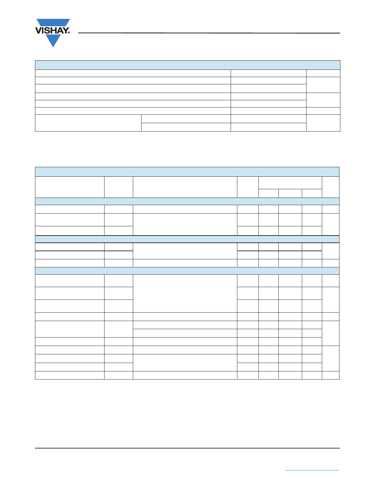
ABSOLUTE MAXIMUM RATINGS
Parameter
Reference V+ to GND
IN, COM, NC, NOa
Continuous Current (Any terminal)
Peak Current (Pulsed at 1 ms, 10 % duty cycle)
Storage Temperature (D suffix)
Power Dissipation (Packages)b
MSOP-8c
SOT23-8c
Limit
Unit
- 0.3 to + 13.5
V
- 0.3 to (V+ + 0.3)
± 10
mA
± 20
- 65 to 150
°C
320
mW
515
Notes:
a. Signals on SX, DX, or INX exceeding V+ or V- will be clamped by internal diodes. Limit forward diode current to maximum current ratings.
b. All leads welded or soldered to PC board.
c. Derate 6.5 mW/°C above 75 °C.
SPECIFICATIONS V+ = 3 V
Parameter
Symbol
Test Conditions
Otherwise Unless Specified
V+ = 3.3 V, ± 10 %, VIN = 0.4 V or 1.8 Ve
Limits
- 40 °C °C to 85 °C
Unit
Temp.a Min.c Typ.b Max.c
Switch On Resistance
Analog Signal Rangee
VANALOG
Full
V-
V+
V
Drain-Source On- Resistance
RON Matchd
Digital Control
R(on)
Ron
V+ = 2.7 V, ICOM = 1 mA, VCOM = 1.5 V
Room
Full
Room
81
100
120
0.4
3.0
Input, High Voltage
Input, Low Voltage
Input Current
VINH
VINL
IINH
V+ Ranges 2.7 to 5 V
Full
1.8
Full
-1
V
0.4
1
µA
Dynamic Characteristics
Break-Before-Maked,g
Turn-On Timed
Turn-Off Timed
tOPEN
tON
tOFF
V+ = 3 V, RL = 300
VNO = VNC = 1.5 V
CL = 35 pF, VIN = 0 V, 3 V
Room
1
Full
Room
Full
Room
Full
60
80
100
ns
14
25
35
Charge Injectiond
Q
CL = 1 nF, RGEN = 0 , Vg = 0 V
Room
0.16
pC
Off-Isolationd
OIRR
CL = 5 pF, RL = 50 , f = 1 MHz
Room
77
CL = 5 pF, RL = 50 , f = 10 MHz
Room
55
dB
Crosstalkd
XTALK
RL = 50 , f = 1 MHz, V+ = 2.5 V
Room
98
Source Off Capacitanced
CNO/NC(off)
f = 1 MHz, VNC/NO = 0 V
Room
7.5
Drain Off Capacitanced
Drain On Capacitanced
CCOM(off)
CCOM(on)
Room
7.8
f = 1 MHz VCOM = 0 V
Room
22
pF
Supply Current
I+
V+ = 3.3 V, VIN = 0 or V+
Room - 1
-1
µA
Notes:
a. Room = 25 °C, Full = as determined by the operating suffix.
b. Typical values are for design aid only, not guaranteed nor subject to production testing.
c. The algebraic convention whereby the most negative value is a minimum and the most positive a maximum, is used in this datasheet.
d. Guarantee by design, not subjected to production test.
e. VIN = input voltage to perform proper function.
f. Guaranteed by 12 V leakage testing, not production tested.
g. Applies for DG9434 only.
Document Number: 72311
www.vishay.com
S11-1029-Rev. B, 23-May-11
3
This document is subject to change without notice.
THE PRODUCTS DESCRIBED HEREIN AND THIS DOCUMENT ARE SUBJECT TO SPECIFIC DISCLAIMERS, SET FORTH AT www.vishay.com/doc?91000
Share Link: 