DG9432 データシートの表示(PDF) - Vishay Semiconductors
部品番号
コンポーネント説明
メーカー
DG9432 Datasheet PDF : 12 Pages
| |||
DG9432, DG9433, DG9434
Vishay Siliconix
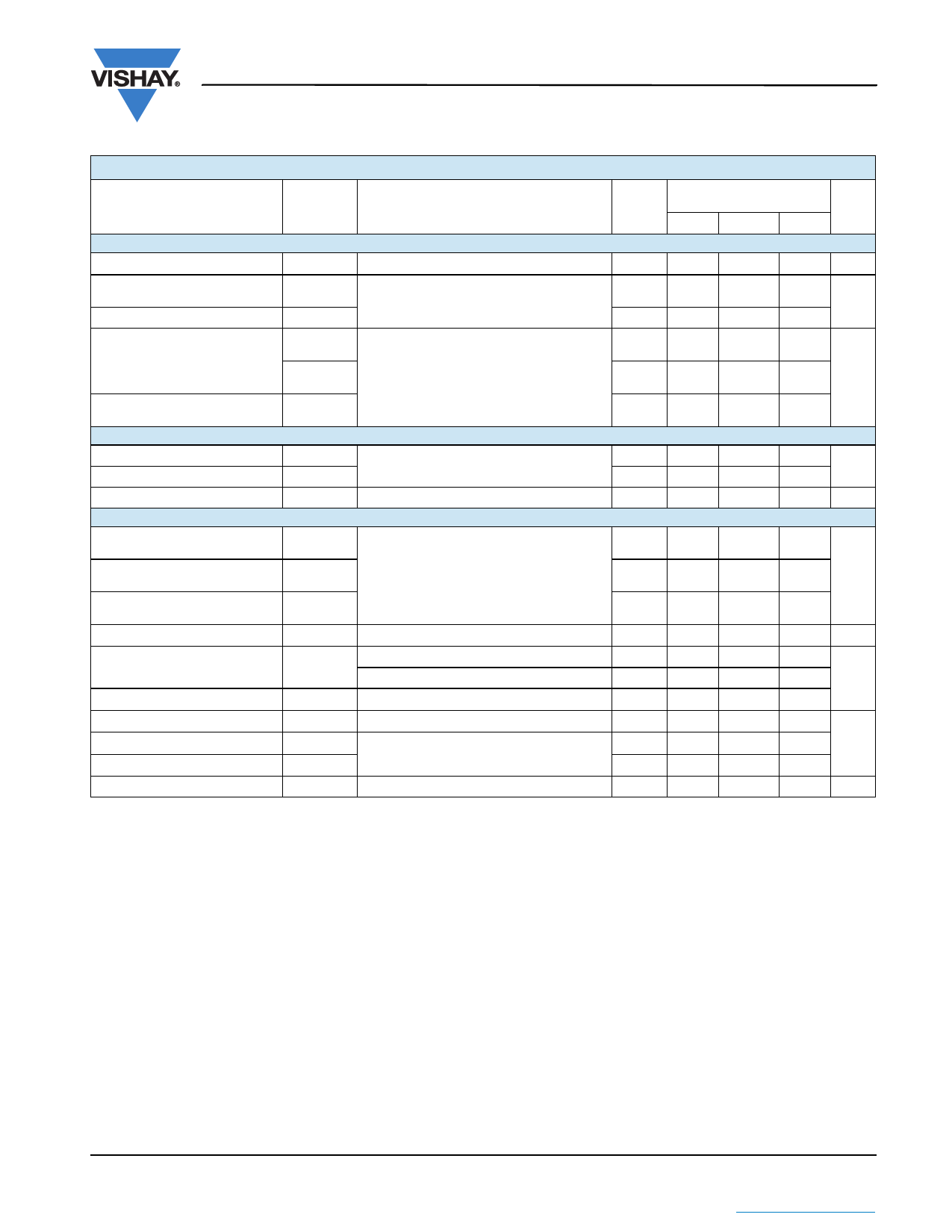
SPECIFICATIONS V+ = 12 V
Parameter
Symbol
Test Conditions
Otherwise Unless Specified
V+ = 12 V, ± 10 %, VIN = 0.8 V or 2.4 Ve
Limits
- 40 °C °C to 85 °C
Unit
Temp.a Min.c Typ.b Max.c
Switch On Resistance
Analog Signal Rangee
VANALOG
Full
V-
V+
V
Drain-Source On-Resistance
RDS(on) Match
R(on)
R(on)
V+ = 10.8 V, ICOM = 1 mA, VCOM = 9 V
Room
Full
Room
19
30
40
0.3
3.0
Switch Off Leakage Currenta
INC/NO(off)
ICOM(off)
V+ = 12 V, VS = 1/11 V, VCOM = 11/1 V
Room - 1
Full
- 10
Room - 1
Full
- 10
0.3
0.3
1
10
1
10
nA
Channel On Leakage Currenta ICOM(on)
Room - 1
0.3
1
Full
- 10
10
Digital Control
Input, High Voltage
Input, Low Voltage
Input Current
Dynamic Characteristics
VINH
VINL
IINH
V+ = 12 V
Full
Full
0.8
-1
2.4
V
1
µA
Break-Before-Maked,g
Turn-On Time
Turn-Off Time
tOPEN
tON
tOFF
V+ = 12 V, RL = 300
VNO = VNC = 8 V
CL = 35 pF, VIN = 0 V, 12 V
Room
1
Full
Room
Full
Room
Full
21
35
40
ns
6
18
25
Charge Injectiond
Off-Isolationd
Crosstalkd
Q
CL = 1 nF, RGEN = 0 , Vg = 0 V, V+ = 5 V Room
0.36
pC
OIRR
CL = 5 pF, RL = 50 , f = 1 MHz
Room
75
CL = 5 pF, RL = 50 , f = 10 MHz
Room
53
dB
XTALK
RL = 50 , f = 1 MHz, V+ = 5 V
Room
96
Source Off Capacitanced
CNO/NC(off)
f = 1 MHz, VNC/NO = 0 V
Room
7.5
Drain Off Capacitanced
Drain On Capacitanced
Supply Current
CCOM(off)
CCOM(on)
I+
f = 1 MHz, VCOM = 0 V
V+ = 12 V, VIN = 0 or V+
Room
7.8
pF
Room
22
Room - 1
-1
µA
Notes:
a. Room = 25 °C, Full = as determined by the operating suffix.
b. Typical values are for design aid only, not guaranteed nor subject to production testing.
c. The algebraic convention whereby the most negative value is a minimum and the most positive a maximum, is used in this datasheet.
d. Guarantee by design, not subjected to production test.
e. VIN = input voltage to perform proper function.
f. Guaranteed by 12 V leakage testing, not production tested.
g. Applies for DG9434 only.
Stresses beyond those listed under “Absolute Maximum Ratings” may cause permanent damage to the device. These are stress ratings only, and functional operation
of the device at these or any other conditions beyond those indicated in the operational sections of the specifications is not implied. Exposure to absolute maximum
rating conditions for extended periods may affect device reliability.
Document Number: 72311
www.vishay.com
S11-1029-Rev. B, 23-May-11
5
This document is subject to change without notice.
THE PRODUCTS DESCRIBED HEREIN AND THIS DOCUMENT ARE SUBJECT TO SPECIFIC DISCLAIMERS, SET FORTH AT www.vishay.com/doc?91000
Share Link: 