DG9432 データシートの表示(PDF) - Vishay Semiconductors
部品番号
コンポーネント説明
メーカー
DG9432 Datasheet PDF : 12 Pages
| |||
DG9432, DG9433, DG9434
Vishay Siliconix
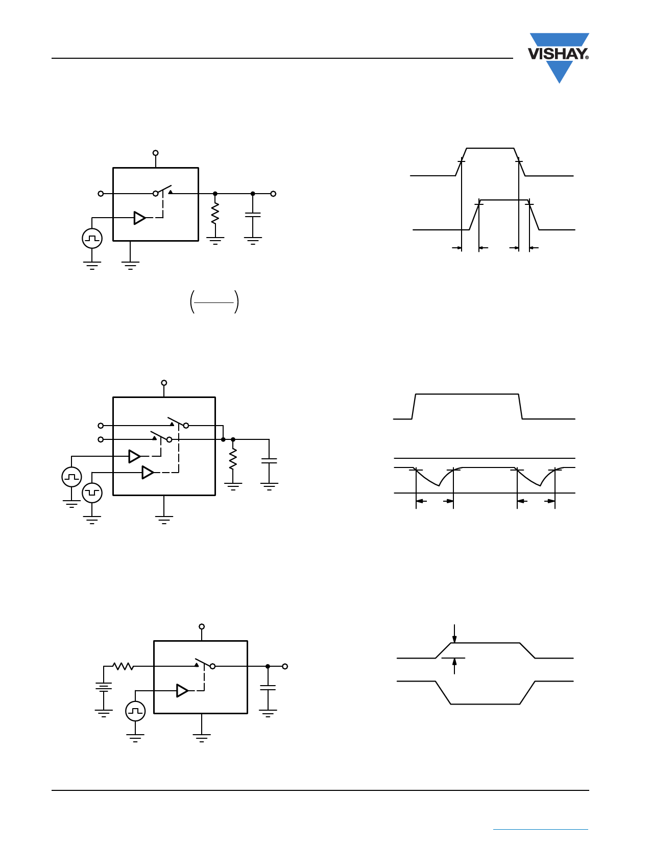
TEST CIRCUITS
Switch
Input
Logi c
Input
V+
V+
NO or NC
COM
IN
GND
0V
Switch Output
VOUT
RL
300 Ω
CL
35 pF
Logic
Input
0V
50 %
Switch
Output
0V
tON
tr < 20 ns
tf < 20 ns
0.9 x VOUT
tOFF
CL (includes fixture and stray capacitance)
VOUT =
VCOM
RL
RL + RON
Logic "1" = Switch On
Logic input waveforms inverted for switches that have
the opposite logic sense.
Figure 1. Switching Time
V+
V+
NO or NC
V1
NO or NC
V2
COM1
COM2
GND
RL
300 Ω
CL
35 pF
Logic
Input
0V
VNC = VNO
VO
Switch 0 V
Output
90 %
tD
CL (includes fixture and stray capacitance)
Figure 2. Break-Before-Make Interval
tr < 5 ns
tf < 5 ns
tD
V+
Vgen
Rgen
+
3V
V+
NC or NO
COM
IN
GND
VOUT
CL
VOUT
ΔVOUT
IN
On
Off
On
Q = ΔVOUT x CL
IN depends on switch configuration: input polarity
determined by sense of switch.
Figure 3. Charge Injection
www.vishay.com
Document Number: 72311
8
S11-1029-Rev. B, 23-May-11
This document is subject to change without notice.
THE PRODUCTS DESCRIBED HEREIN AND THIS DOCUMENT ARE SUBJECT TO SPECIFIC DISCLAIMERS, SET FORTH AT www.vishay.com/doc?91000
Share Link: 