DG9432DQ データシートの表示(PDF) - Vishay Semiconductors
部品番号
コンポーネント説明
メーカー
DG9432DQ Datasheet PDF : 10 Pages
| |||
DG9432/9433/9434
Vishay Siliconix
New Product
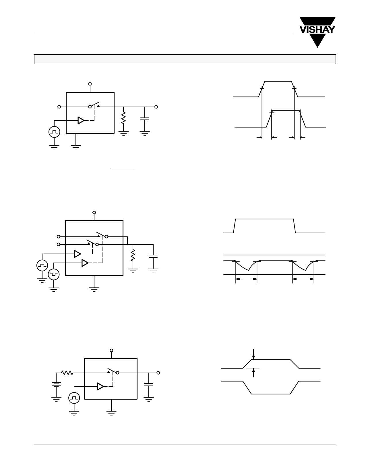
TEST CIRCUITS
Switc
h
Input
Logi
c
Input
V+
V+
NO or NC
COM
IN
GND
0V
Switch Output
VOUT
RL
300 W
CL
35 pF
CL (includes fixture and stray capacitance)
ǒ Ǔ VOUT + VCOM
RL
RL ) RON
Logic
Input
0V
50%
tr t
20 ns
tf t 20 ns
Switch
Output
0V
tON
0.9 x VOUT
tOFF
Logic “1” = Switch On
Logic input waveforms inverted for switches that have
the opposite logic sense.
FIGURE 1. Switching Time
V+
V+
NO or NC
V1
NO or NC
V2
COM1
COM2
GND
RL
300 W
CL
35 pF
Logic
Input
0V
VNC = VNO
VO
Switch 0 V
Output
90%
tD
CL (includes fixture and stray capacitance)
FIGURE 2. Break-Before-Make Interval
tr <5 ns
tf <5 ns
tD
V+
Vgen
Rgen
+
3V
V+
NC or NO
COM
IN
GND
www.vishay.com
8
VOUT
CL
VOUT
DVOUT
IN
On
Off
On
Q = DVOUT x CL
IN depends on switch configuration: input polarity
determined by sense of switch.
FIGURE 3. Charge Injection
Document Number: 72311
S-31643—Rev. A, 01-Aug-03
Share Link: 