UPB1508GV データシートの表示(PDF) - NEC => Renesas Technology
部品番号
コンポーネント説明
メーカー
UPB1508GV Datasheet PDF : 12 Pages
| |||
µPB1508GV
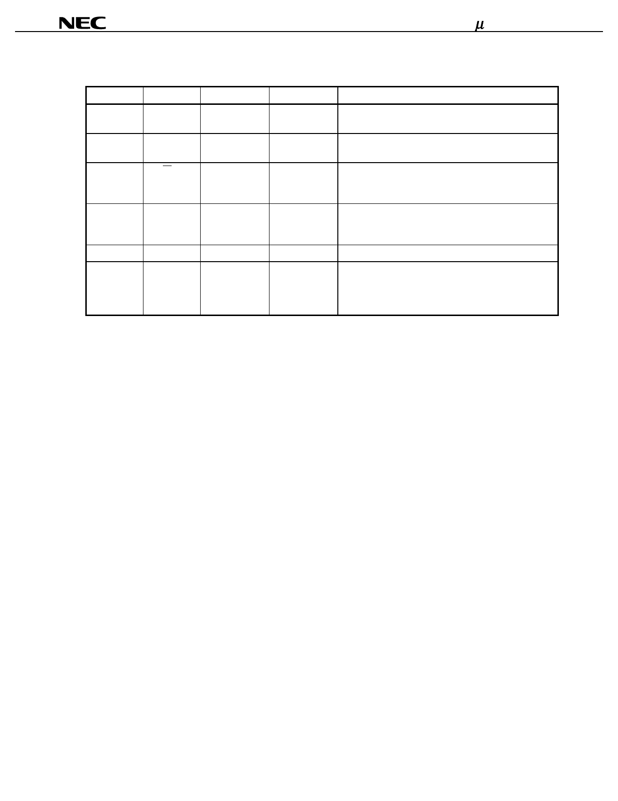
PIN EXPLANATION
Pin No.
1
2
3
4, 5
6, 8
7
Symbol
VCC
IN
IN
GND
NC
OUT
Applied voltage
4.5 to 5.5
0
PIN voltage
1.7 to 4.95
1.7 to 4.95
1.0 to 4.7
Functions and explanation
Power supply pin. This pin must be equipped with bypass
capacitor (eg 1 000 pF) to minimize ground impedance.
Signal input pin. This pin should be coupled to signal
source with capacitor (eg 1 000 pF) for DC cut.
Signal input bypass pin. This pin must be equipped with
bypass capacitor (eg 1 000 pF) to minimize ground
impedance.
Ground pin. Ground pattern on the board should be
formed as wide as possible to minimize ground
impedance.
Non connection pins. These pins should be opened.
Divided frequency output pin. This pin is designed as
emitter follower output. This pin can be connected to
input of prescaler within PLL synthesizer through DC cut
capacitor.
3
Share Link: 