LA4585M データシートの表示(PDF) - SANYO -> Panasonic
部品番号
コンポーネント説明
メーカー
LA4585M Datasheet PDF : 5 Pages
| |||
LA4585M
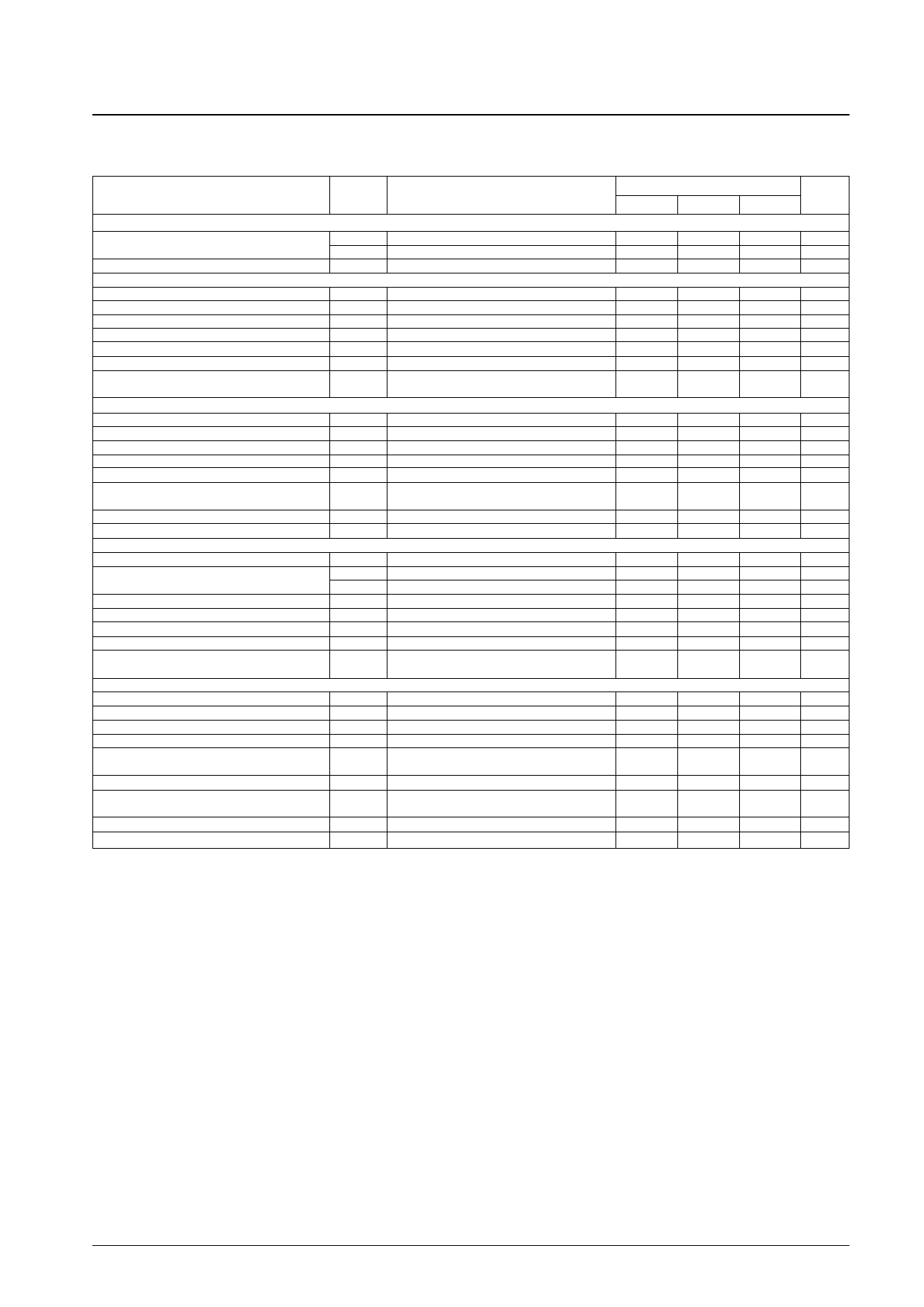
Operating Characteristics at Ta = 25°C, VCC = 3.0 V, fi = 1 kHz, 0.775 = 0 dBm, preamplifier RL = 10 kΩ,
low boost, power amplifier RL = 10 Ω
Parameter
Symbol
Conditions
[PRE + LOW BOOST + PVSS + PWR]
Quiescent current
Voltage gain (closed loop)
[PRE AMP]
ICCO1
ICCO2
VGT
Rg = 2.2 kΩ, low boost off, PVSS off
Rg = 2.2 kΩ, low boost on, PVSS on
VO = –5 dBm
Voltage gain (open loop)
Voltage gain (closed loop)
Maximum output voltage
Total harmonic distortion
Equivalent input noise voltage
Crosstalk
VG0
VG1
VO max1
THD1
VNI
CT1
VO = –5 dBm
VO = –5 dBm
THD = 1 %, VCC = 1.8 V
VO = 0.2 V, VG = 40 dB/NAB
Rg = 2.2 kΩ, BPF = 20 Hz to 20 kHz
Rg = 2.2 kΩ, TUNE 1 kHz
Ripple rejection ratio
SVRR
Rg = 2.2 kΩ, VCC = 1.8 V, Vr = –20 dBm,
fr = 100 Hz
[POWER AMP]
Output voltage
Voltage gain
Total harmonic distortion
Interchannel crosstalk
Output noise voltage
Ripple rejection ratio
Input resistance
PO
VG2
THD2
CT2
VNO1
Rr2
Ri
THD = 10 %
VO = –5 dBm
PO = 1 mW
VO = –5 dBm, RV = 0 Ω
RV = 0 Ω, BPF = 20 Hz to 20 kHz
RV = 0 Ω, Vr = –20 dBm,
fr = 100 Hz, VCC = 1.8 V
DC offset voltage
[LOW BOOST]
VODC OFF Between pin 6 and pins 4 and 8
Voltage gain
VG3 Vi = –30 dBm, boost on/off
Boost*
BST1 ViBST = –30 dBm, f = 100 Hz, boost on
BST2 ViBST = –30 dBm, f = 10 kHz, boost on
Maximum output voltage
VO max2 THD = 1%, boost on
Total harmonic distortion
THD3 VO = 0.1 V, boost on
Interchannel crosstalk
CT3 VO = –20 dBm, Rg = 0, boost on
Output noise voltage
VNO2 Rg = 0, BPF = 20 Hz to 20 kHz, boost on
Ripple rejection ratio
Rr3
Rg = 0, fR = 100 Hz, VR = –20 dBm,
VCC = 1.8 V, boost on
[LOW BOOST + PVSS + POWER] The following items are measured at an RV of 10 kΩ maximum.
Voltage gain
VG4 Vi = –40 dBm, f = 1 kHz, boost off/on
LOW BOOST output voltage
LOW BOOST output voltage
LOW BOOST total harmonic distortion
VO1
VO2
THD4
Vi = –43 dBm, f = 100 Hz, boost on
Vi = –28 dBm, f = 100 Hz, boost on
Vi = –40 dBm, f = 100 Hz, boost on
Output noise voltage
VNO3
Rg = 0, CCIR-ARM, boost off, with the power
input switch K18 set to B.
PVSS voltage
PVSS width
VO3
WPVSS
Vi = –40 dBm, PVSS 2
The input amplitude between the start point and
the point where the output is +4 dB. PVSS on
PVSS harmonic distortion
THD5 Vi = –40 dBm, PVSS 2
PVSS start input level
VOPi PVSS 2
Ratings
min
typ
12
15
12
15
62
64
70
83
40
0.1
0.2
0.05
1.3
60
80
40
50
23
34
27
29
0.4
30
40
25
45
55
22
30
–90
–2.3
–3.8
11.2
14.7
7.0
8.5
0.25
0.4
0.1
25
32
2.0
45
53
22
24
0.13
0.23
0.25
0.40
0.5
–88
–85
–40
–37
30
40
0.5
–67
–63
Unit
max
21 mA
21
µA
67
dB
dB
dB
V
0.5
%
2.0
µV
dB
dB
mW
32
dB
1.0
%
dB
40
µV
dB
38
kΩ
+90 mV
–5.3
dB
18.2
dB
10
dB
V
0.5
%
dB
5.0
µV
dB
27
dB
0.33
V
0.55
V
1.2
%
–82 dBm
–34 dBm
dB
1.2
%
–59 dBm
Note: *The amount of boost for a 1-kHz input.
No. 5661-2/5
Share Link: 