EL2125CS(2005) データシートの表示(PDF) - Intersil
部品番号
コンポーネント説明
メーカー
EL2125CS Datasheet PDF : 15 Pages
| |||
EL2125
Absolute Maximum Ratings (TA = 25°C)
VS+ to VS- . . . . . . . . . . . . . . . . . . . . . . . . . .
33V
Continuous Output Current . . . . . . . . . . . . . . . . . . . . . . . . . . . 40mA
Any Input . . . . . . . . . . . . . . . . . . . . . . . . . . VS- - 0.3V to VS+ + 0.3V
Power Dissipation . . . . . . . . . . . . . . . . . . . . . . . . . . . . . See Curves
Ambient Operating Temperature . . . . . . . . . . . . . . . .-45°C to +85°C
Storage Temperature . . . . . . . . . . . . . . . . . . . . . . . -65°C to +150°C
Maximum Die Junction Temperature . . . . . . . . . . . . . . . . . . . +150°C
CAUTION: Stresses above those listed in “Absolute Maximum Ratings” may cause permanent damage to the device. This is a stress only rating and operation of the
device at these or any other conditions above those indicated in the operational sections of this specification is not implied.
IMPORTANT NOTE: All parameters having Min/Max specifications are guaranteed. Typical values are for information purposes only. Unless otherwise noted, all tests
are at the specified temperature and are pulsed tests, therefore: TJ = TC = TA
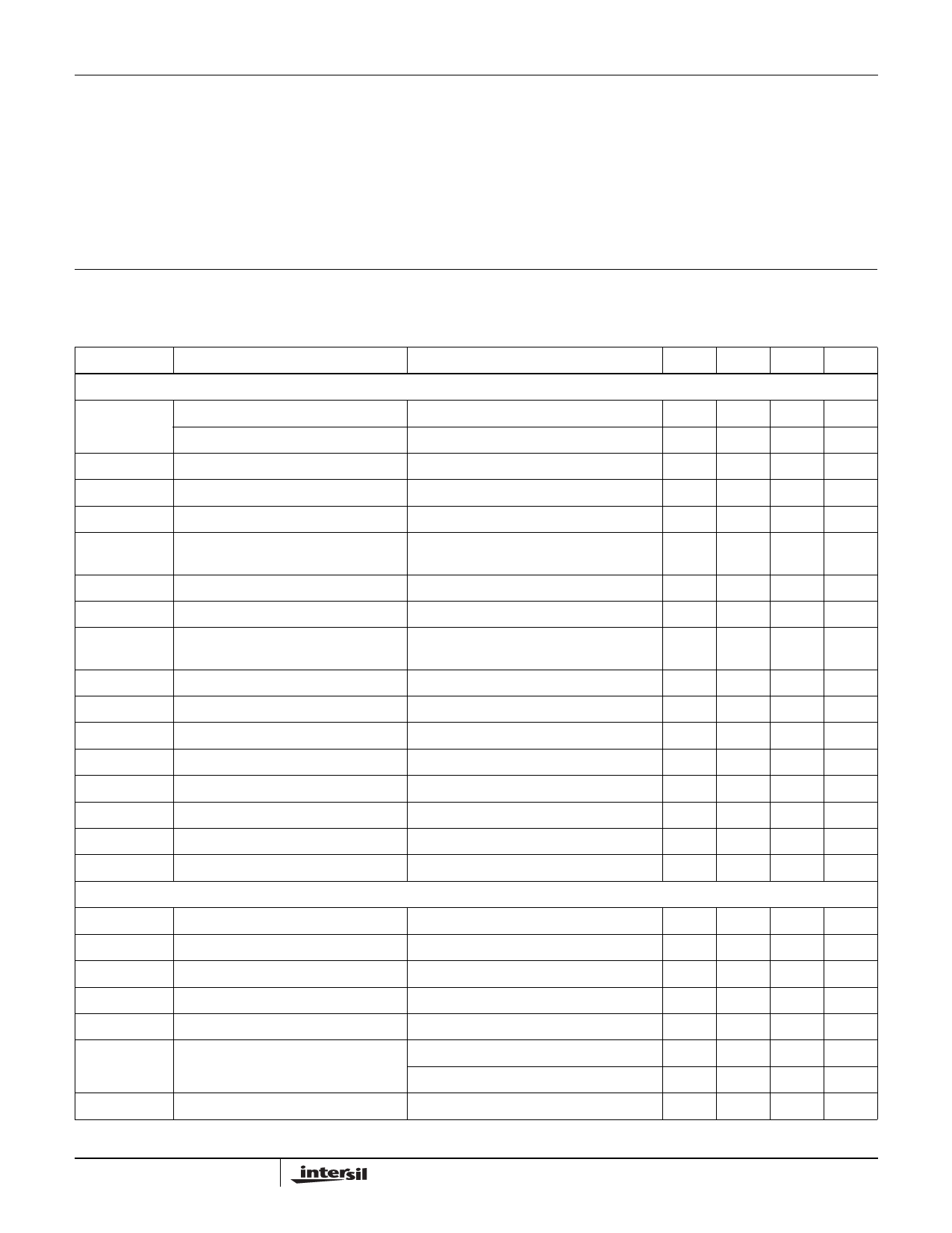
Electrical Specifications VS = ±5V, TA = 25°C, RF = 180Ω, RG = 20Ω, RL = 500Ω unless otherwise specified.
PARAMETER
DESCRIPTION
CONDITIONS
MIN TYP
DC PERFORMANCE
VOS
Input Offset Voltage (SO8)
0.2
Input Offset Voltage (SOT23-5)
TCVOS
IB
IOS
TCIB
Offset Voltage Temperature Coefficient
Input Bias Current
Input Bias Current Offset
Input Bias Current Temperature
Coefficient
1.8
-30
-22
0.4
0.09
CIN
AVOL
PSRR
Input Capacitance
Open Loop Gain
Power Supply Rejection Ratio
(Note 1)
2.2
80
87
80
97
CMRR
Common Mode Rejection Ratio
at CMIR
80
106
CMIR
Common Mode Input Range
-4.6
VOUTH
Output Voltage Swing High
VOUTL
Output Voltage Swing Low
VOUTH2
Output Voltage Swing High
VOUTL2
Output Voltage Swing Low
IOUT
Output Short Circuit Current (Note 2)
IS
Supply Current
AC PERFORMANCE - RG = 20Ω, CL = 5pF
BW
-3dB Bandwidth
No load, RF = 1kΩ
No load, RF = 1kΩ
RL = 100Ω
RL = 100Ω
3.5
3.65
-3.87
3
3.3
-3.5
80
100
10.1
175
BW ±0.1dB
±0.1dB Bandwidth
34
BW ±1dB
±1dB Bandwidth
150
Peaking
Peaking
0.4
SR
Slew Rate
VOUT = 2VP-P, measured at 20% to 80%
150
185
OS
Overshoot, 4VP-P Output Square Wave Positive
0.6
Negative
2.7
tS
Settling Time to 0.1% of ±1V Pulse
VN
Voltage Noise Spectral Density
10kHz
42
0.83
MAX UNIT
2
mV
3
mV
µV/°C
µA
2
µA
µA/°C
pF
dB
dB
dB
3.8
V
V
-3.7
V
V
-3
V
mA
11
mA
MHz
MHz
MHz
dB
V/µs
%
%
ns
nV/√Hz
2
FN7045.2
April 21, 2005
Share Link: 