EL2257 データシートの表示(PDF) - Intersil
部品番号
コンポーネント説明
メーカー
EL2257 Datasheet PDF : 17 Pages
| |||
EL2257
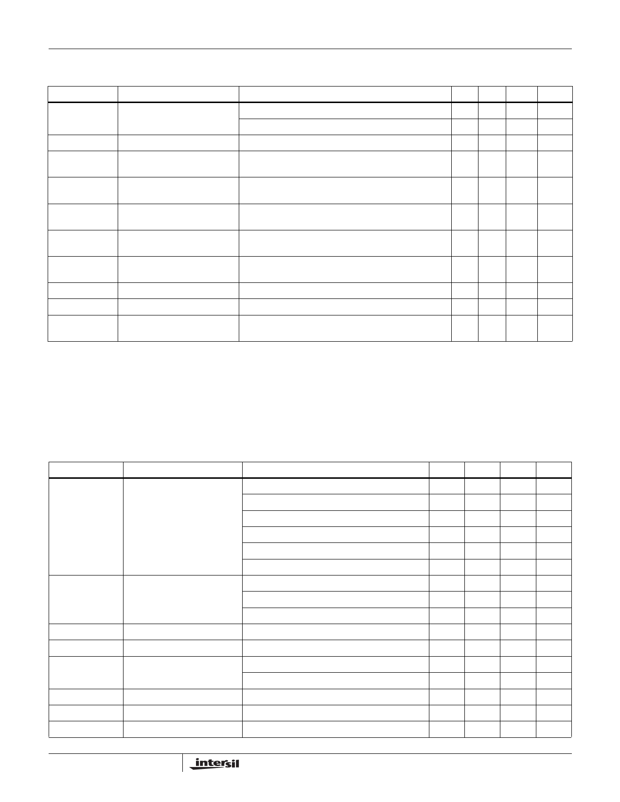
DC Electrical Specifications VS = +5V, GND = 0V, TA = 25°C, VCM = 1.5V, VOUT = 1.5V, VCLAMP = +5V, VENABLE = +5V, unless
otherwise specified. (Continued)
PARAMETER
DESCRIPTION
CONDITIONS
MIN TYP MAX UNIT
IOUT
IOUT,OFF
VIH-EN
Output Current (Note 1)
VS = ±5V, AV = 1, RL = 10Ω to 0V
VS = ±5V, AV = 1, RL = 50Ω to 0V
Output Current - Disabled
VENABLE = 0.5V
ENABLE Pin Voltage for Power- Relative to GND pin
up
±75 ±100
mA
±60
mA
0
20
µA
2.0
V
VIL-EN
ENABLE Pin Voltage for Shut- Relative to GND pin
down
0.5
V
IIH-EN
ENABLE Pin Input Current -
High(Note 2)
VS = VCLAMP = 12V, VENABLE = 12V
340 410
µA
IIL-EN
ENABLE Pin Input Current - Low VS = VCLAMP = 12V, VENABLE = 0.5V
(Note 2)
0
1
µA
VOR-CL
Voltage Clamp Operating
Range (Note 3)
Relative to GND pin
1.2
VOP
V
VACC-CL
IIH-CL
IIL-CL
CLAMP Accuracy (Note 4)
VIN = 4V, RL = 1kΩ to GND, VCLAMP = 1.5V and 3.5V
-250 100 250
mV
CLAMP Pin Input Current - High VS = VCLAMP = 12V
12 25
µA
CLAMP Pin Input Current - Low VS = 12V, VCLAMP = 1.2V
(per amp)
-30 -15
µA
NOTES:
1. Internal short circuit protection circuitry has been built into the EL2257. See the Applications section.
2. If the disable feature is not desired, tie the ENABLE pins to the VS pin, or apply a logic high level to the ENABLE pins.
3. The maximum output voltage that can be clamped is limited to the maximum positive output Voltage, or VOP. Applying a voltage higher than VOP
inactivates the clamp. If the clamp feature is not desired, either tie the CLAMP pin to the VS pin, or simply let the CLAMP pin float.
4. The clamp accuracy is affected by VIN and RL. See the Typical Curves Section and the Clamp Accuracy vs VIN and RL curve.
Closed Loop AC Electrical Specifications VS = +5V, GND = 0V, TA = 25°C, VCM = +1.5V, VOUT = +1.5V, VCLAMP = +5V, VENABLE
= +5V, AV = +1, RF = 0Ω, RL = 150Ω to GND pin unless otherwise specified. (Note 1)
PARAMETER
DESCRIPTION
CONDITIONS
MIN TYP MAX UNIT
BW
BW
GBWP
PM
SR
tR,tF
OS
-3dB Bandwidth
(VOUT = 400mVP-P)
±0.1dB Bandwidth
(VOUT = 400mVP-P)
Gain Bandwidth Product
Phase Margin
Slew Rate
Rise Time, Fall Time
Overshoot
VS = 5V, AV = 1, RF = 0Ω
VS = 5V, AV = -1, RF = 500Ω
VS = 5V, AV = 2, RF = 500Ω
VS = 5V, AV = 10, RF = 500Ω
VS = 12V, AV = 1, RF = 0Ω
VS = 3V, AV = 1, RF = 0Ω
VS = 12V, AV = 1, RF = 0Ω
VS = 5V, AV = 1, RF = 0Ω
VS = 3V, AV = 1, RF = 0Ω
VS = 12V, @ AV = 10
RL = 1kΩ, CL = 6pF
VS = 10V, RL = 150Ω, VOUT = 0V to 6V
VS = 5V, RL = 150Ω, VOUT = 0V to +3V
±0.1V step
±0.1V step
125
60
60
6
150
100
25
30
20
60
55
200
275
300
2.8
10
MHz
MHz
MHz
MHz
MHz
MHz
MHz
MHz
MHz
MHz
°
V/µs
V/µs
ns
%
tPD
Propagation Delay
±0.1V step
3.2
ns
3
Share Link: 