5108IS(2006) データシートの表示(PDF) - Intersil
部品番号
コンポーネント説明
メーカー
5108IS Datasheet PDF : 13 Pages
| |||
EL5108, EL5308
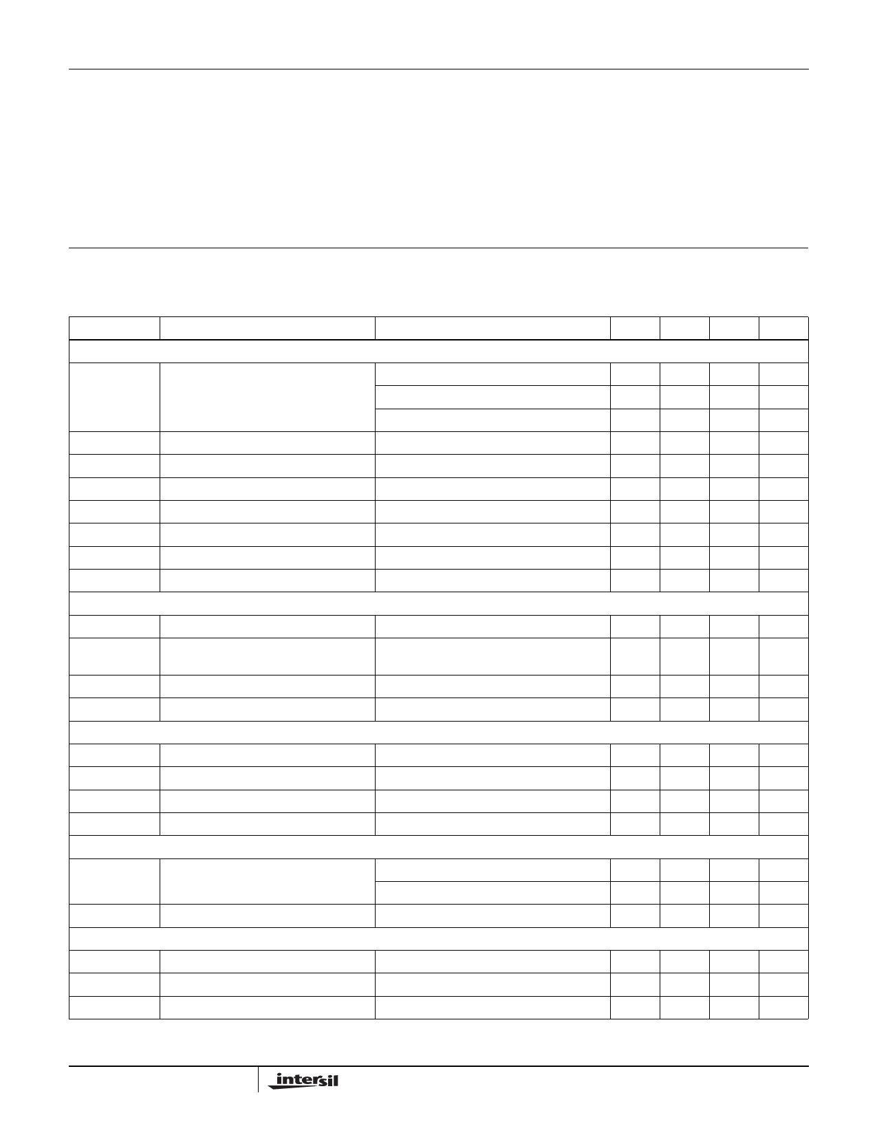
Absolute Maximum Ratings (TA = 25°C)
Supply Voltage between VS+ and VS- . . . . . . . . . . . . . . . . . . . 13.2V
Maximum Continuous Output Current . . . . . . . . . . . . . . . . . . . 50mA
Maximum Slewrate from VS+ to VS- . . . . . . . . . . . . . . . . . . . . 1V/µs
Operating Junction Temperature . . . . . . . . . . . . . . . . . . . . . . . 125°C
Power Dissipation . . . . . . . . . . . . . . . . . . . . . . . . . . . . . See Curves
Pin Voltages. . . . . . . . . . . . . . . . . . . . . . . . . VS- -0.5V to VS+ +0.5V
Storage Temperature . . . . . . . . . . . . . . . . . . . . . . . .-65°C to +150°C
Ambient Operating Temperature . . . . . . . . . . . . . . . .-40°C to +85°C
CAUTION: Stresses above those listed in “Absolute Maximum Ratings” may cause permanent damage to the device. This is a stress only rating and operation of the
device at these or any other conditions above those indicated in the operational sections of this specification is not implied.
IMPORTANT NOTE: All parameters having Min/Max specifications are guaranteed. Typical values are for information purposes only. Unless otherwise noted, all tests
are at the specified temperature and are pulsed tests, therefore: TJ = TC = TA
Electrical Specifications VS+ = +5V, VS- = -5V, RL = 150Ω, TA = 25°C unless otherwise specified.
PARAMETER
DESCRIPTION
CONDITIONS
MIN
AC PERFORMANCE
BW
-3dB Bandwidth
BW1
0.1dB Bandwidth
SR
Slew Rate
tS
0.1% Settling Time
eN
Input Voltage Noise
iN
Input Current Noise
dG
Differential Gain Error (Note 1)
dP
Differential Phase Error (Note 1)
DC PERFORMANCE
AV = +1
AV = -1
AV = +2
AV = +2
VO = -2.5V to +2.5V, AV = +2
VOUT = -2.5V to +2.5V, AV = +2
f = 2kHz
AV = +2
AV = +2
3500
VOS
Offset Voltage
-8
TCVOS
Input Offset Voltage Temperature
Coefficient
Measured from TMIN to TMAX
AE
Gain Error
RF, RG
Internal RF and RG
INPUT CHARACTERISTICS
VO = -3V to +3V, RL = 150Ω
CMIR
Common Mode Input Range
±3
+IIN
+ Input Current
RIN
Input Resistance
CIN
Input Capacitance
OUTPUT CHARACTERISTICS
at IN+
VO
Output Voltage Swing
RL = 150Ω to GND
±3.6
RL = 1kΩ to GND
±3.8
IOUT
Output Current
RL = 10Ω to GND
100
SUPPLY
ISON
ISOFF
PSRR
Supply Current - Enabled (per amplifier) No load, VIN = 0V
Supply Current - Disabled (per amplifier) No load, VIN = 0V
Power Supply Rejection Ratio
DC, VS = ±4.75V to ±5.25V
3.18
TYP
440
445
450
40
4500
10
2
12
0.01
0.01
+3
5
0.7
325
±3.3
2
0.7
1
±3.8
±4.0
135
3.7
9
75
MAX UNIT
MHz
MHz
MHz
MHz
V/µs
ns
nV/√Hz
pA/√Hz
%
°
+8
mV
µV/°C
2.5
%
Ω
V
8
µA
MΩ
pF
V
V
mA
4.35
mA
25
µA
dB
3
FN7358.5
June 15, 2006
Share Link: 