7156CS データシートの表示(PDF) - Intersil
部品番号
コンポーネント説明
メーカー
7156CS Datasheet PDF : 10 Pages
| |||
EL7156
Absolute Maximum Ratings (TA = +25°C)
Supply Voltage (VS+ to VS-) . . . . . . . . . . . . . . . . . . . . . . . . . . .+18V
Input Voltage . . . . . . . . . . . . . . . . . . . . . . . . . . . VS- -0.3V, VS +0.3V
Continuous Output Current . . . . . . . . . . . . . . . . . . . . . . . . . . 200mA
Storage Temperature Range . . . . . . . . . . . . . . . . . .-65°C to +150°C
Thermal Information
Ambient Operating Temperature . . . . . . . . . . . . . . . .-40°C to +85°C
Operating Junction Temperature . . . . . . . . . . . . . . . . . . . . . . +125°C
Power Dissipation . . . . . . . . . . . . . . . . . . . . . . . . . . . . . . see curves
Pb-free reflow profile . . . . . . . . . . . . . . . . . . . . . . . . . .see link below
http://www.intersil.com/pbfree/Pb-FreeReflow.asp
*Pb-free PDIPs can be used for through hole wave solder
processing only. They are not intended for use in Reflow solder
processing applications.
CAUTION: Stresses above those listed in “Absolute Maximum Ratings” may cause permanent damage to the device. This is a stress only rating and operation of the
device at these or any other conditions above those indicated in the operational sections of this specification is not implied.
IMPORTANT NOTE: All parameters having Min/Max specifications are guaranteed. Typical values are for information purposes only. Unless otherwise noted, all tests
are at the specified temperature and are pulsed tests, therefore: TJ = TC = TA
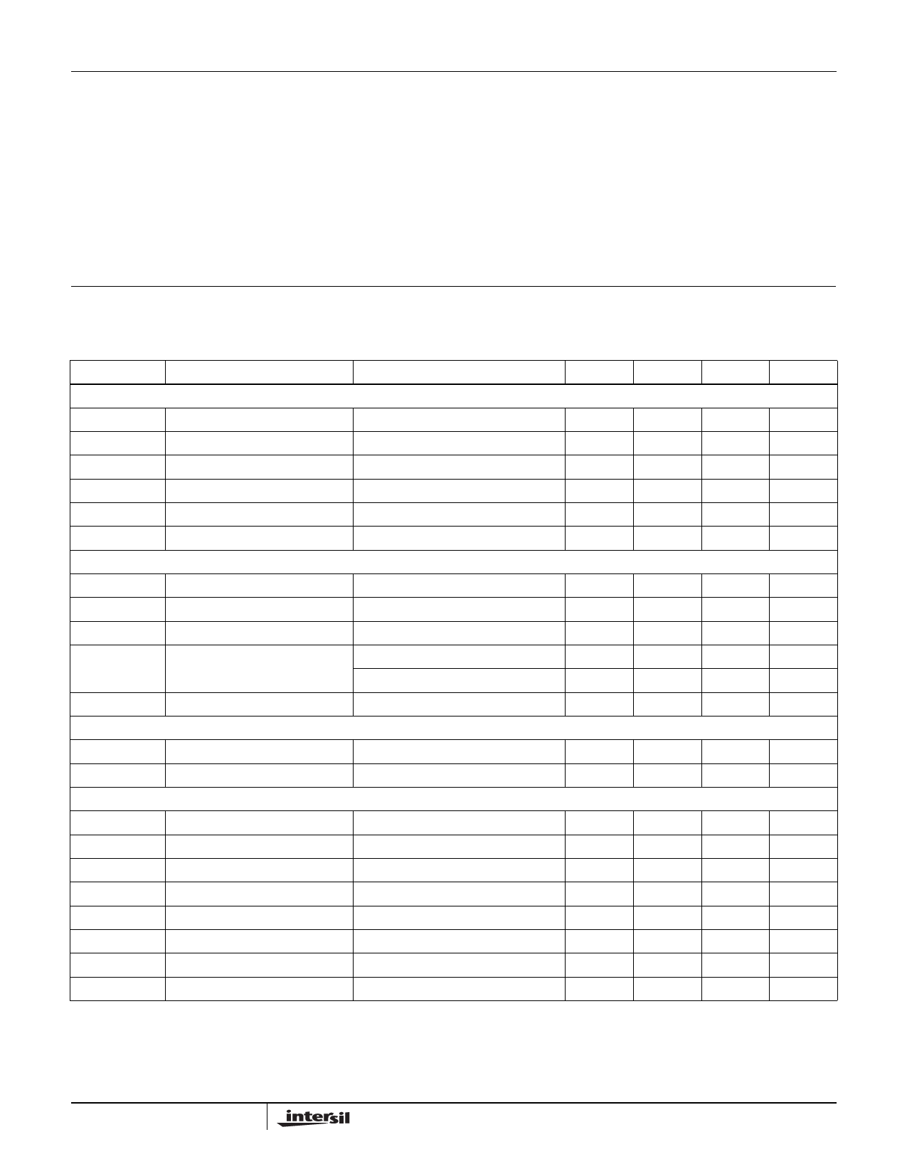
Electrical Specifications VS+ = +15V, VH = +15V, VL = 0V, VS- = 0V, TA = +25°C, unless otherwise specified.
PARAMETER
DESCRIPTION
CONDITION
MIN
TYP
INPUT
VIH
IIH
VIL
IIL
CIN
RIN
OUTPUT
Logic ‘1’ Input Voltage
Logic ‘1’ Input Current
Logic ‘0’ Input Voltage
Logic ‘0’ Input Current
Input Capacitance
Input Resistance
VIH = VS+
VIL = 0V
2.4
0.1
0.1
3.5
50
ROVH
ON-Resistance VH to OUT
IOUT = -200 mA
2.7
ROVL
ON-Resistance VL to OUT
IOUT = +200 mA
3.5
IOUT
Output Leakage Current
OE = 0V, OUT = VH/VL
0.1
IPK
Peak Output Current
Source
3.5
(linear resistive operation)
Sink
3.5
IDC
Continuous Output Current
Source/Sink
200
POWER SUPPLY
IS
Power Supply Current
Inputs = VS+
1.3
IVH
Off Leakage at VH and VL
VH, VL = 0V
4
SWITCHING CHARACTERISTICS
tR
Rise Time
CL = 2000pF
14.5
tF
Fall Time
CL = 2000pF
15
tRFΔ
tR, tF Mismatch
CL = 2000pF
0.5
td-1
Turn-Off Delay Time
CL = 2000pF
9.5
td-2
Turn-On Delay Time
CL = 2000pF
10
tdΔ
td-1-td-2 Mismatch
CL = 2000pF
0.5
td-3
Three-state Delay Enable
10
td-4
Three-state Delay Disable
10
MAX
10
0.8
10
4.5
5.5
10
3
10
UNIT
V
µA
V
µA
pF
MΩ
Ω
Ω
µA
A
A
mA
mA
µA
ns
ns
ns
ns
ns
ns
ns
ns
2
FN7280.3
May 2, 2007
Share Link: 