FAN4801 データシートの表示(PDF) - Fairchild Semiconductor
部品番号
コンポーネント説明
メーカー
FAN4801 Datasheet PDF : 17 Pages
| |||
AN-8027
(Design Example) Setting the crossover frequency
as 22Hz:
CVC1
=
GMV ⋅ I BOUT ⋅ KMAX
5 ⋅ CBOUT ⋅ (2π fVC )2
⋅ 2.5
VBOUT
=
70 ×10−6 ⋅ 0.9 ⋅1.27
5 ⋅ 270 ×10−6 ⋅ (2π ⋅ 22)2
⋅
2.5
387
=
20nF
RVC
=
2π ⋅
1
fVC
⋅ CVC1
=
1
2π ⋅ 22 ⋅ 20 ×10−9
= 362kΩ
Setting the pole of the compensator at 120Hz:
CVC 2
=
1
2π ⋅ fVP ⋅ RVC
=
1
2π ⋅120 ⋅ 362 ×103
= 3.7nF
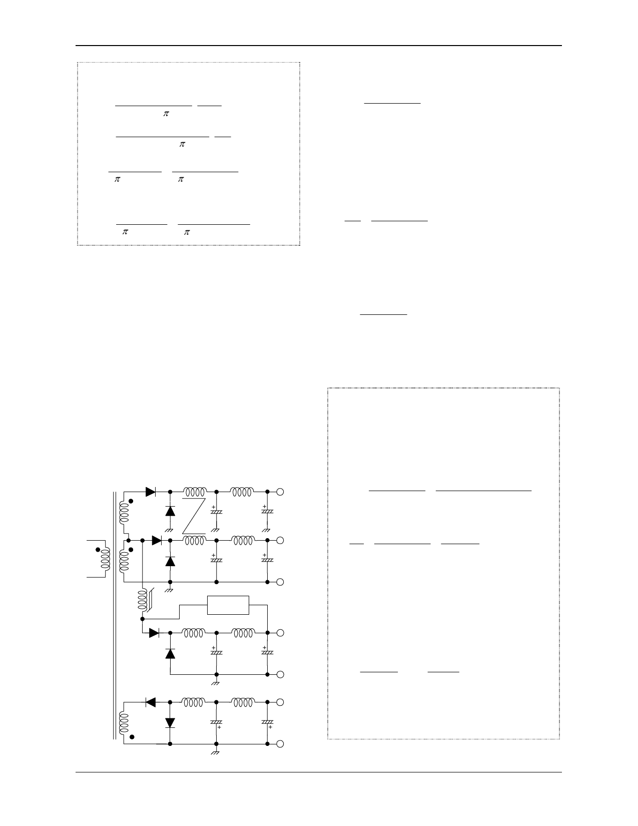
[STEP-10] Transformer Design for PWM
Stage
Figure 19 shows the typical secondary-side circuit of
forward converter for multi-output of PC power application.
A common technique for winding multiple outputs with the
same polarity sharing a common ground is to stack the
secondary windings instead of winding each output
winding separately. This approach improves the load
regulation of the stacked outputs. The winding NS1 in
Figure 19 must be sized to accommodate its output current,
plus the current of the output (+12V) stacked on top of it.
To get tight regulation of 3.3V output, magnetic amplifier
(MAG-AMP) is used. The saturable core of MAG-AMP
prevents the diode DREC from fully conducting by
introducing high impedance until it is saturated. This
allows the effective duty cycle of VREC to be controlled to
be regulated the output voltage.
Additiona
l LC filter
+12V
NS
2
Np
NS
1
Additiona
l LC filter
+5V
MAG
AMP
DREC
+
VREC
-
MAG AMP
Control
+3.3
V
Additiona
l LC filter
NS
Additiona
l LC filter
-12V
3
Once the core for the transformer is determined, the
minimum number of turns for the transformer primary-side
to avoid saturation is given by:
N P MIN
= VBOUT MIN DMAX
Ae fSW ΔB
(44)
where Ae is the cross sectional area of the core in m2, fSW is
the switching frequency, and ΔB is the maximum flux
density swing in Tesla for normal operation. ΔB is typically
0.2-0.3 T for most power ferrite cores in the case of a
forward converter.
The turn ratio between the primary-side and secondary-side
winding for the first output is determined by:
n = NP = VBOUT MIN DMAX
NS1
(VO1 + VF1 )
(45)
where VF is the diode forward-voltage drop.
Next, determine the proper integer for NS1 resulting in Np
larger than Npmin. Once the number of turns of the first
output is determined, the number of turns of other output
(n-th output) can be determined by:
NS(n)
=
VO(n) + VF (n)
VO1 + VF1
⋅ NS1
(46)
The golden ratio between the secondary-side windings for
the best regulation of 3.3V, 5V, and 12V is known as
2:3:7.
(Design Example) The minimum PFC output voltage
is 310V and the maximum duty cycle of PWM
controller is 50%. By adding 5% margin to the
maximum duty cycle, DMAX=0.45 is used for
transformer design. Assuming ERL35 (Ae=107mm2)
core is used and ΔB=0.28, the minimum turns for the
transformer primary side is obtained as:
N PMIN
= VBOUT MIN DMAX
Ae fSW ΔB
=
310 ⋅ 0.45
107 ×10−6 ⋅ 65×103
⋅ 0.28
=
72
The turns ratio for 5V output is obtained as:
n = NP
=
V MIN
BOUT
DMAX
= 310 ⋅ 0.45 = 25.6
NS
(VO + VF ) (5 + 0.45)
The number of turns for the primary-side winding is
determined as:
N p = n ⋅ NS1 = 2 × 25.6 = 51.2 < NPMIN
N p = n ⋅ NS1 = 3× 25.6 = 76.8 > NPMIN ∴ NS1 = 3
Then, the turns ratio for 12V output is obtained as:
NS2
=
VO 2
VO1
+ VF 2
+ VF1
⋅
NS1
=
12 + 0.7
5 + 0.45
⋅3 =
6.99
≅
7
Therefore, the number of turns for each winding is
obtained as:
Np=78, NS1=3, NS2=7 (3+4 stack) and NS3=7.
Figure 19. Typical Secondary-Side Circuit
© 2009 Fairchild Semiconductor Corporation
Rev. 1.0.0 • 8/26/09
11
www.fairchildsemi.com
Share Link: 