FAN4860 データシートの表示(PDF) - Fairchild Semiconductor
部品番号
コンポーネント説明
メーカー
FAN4860 Datasheet PDF : 15 Pages
| |||
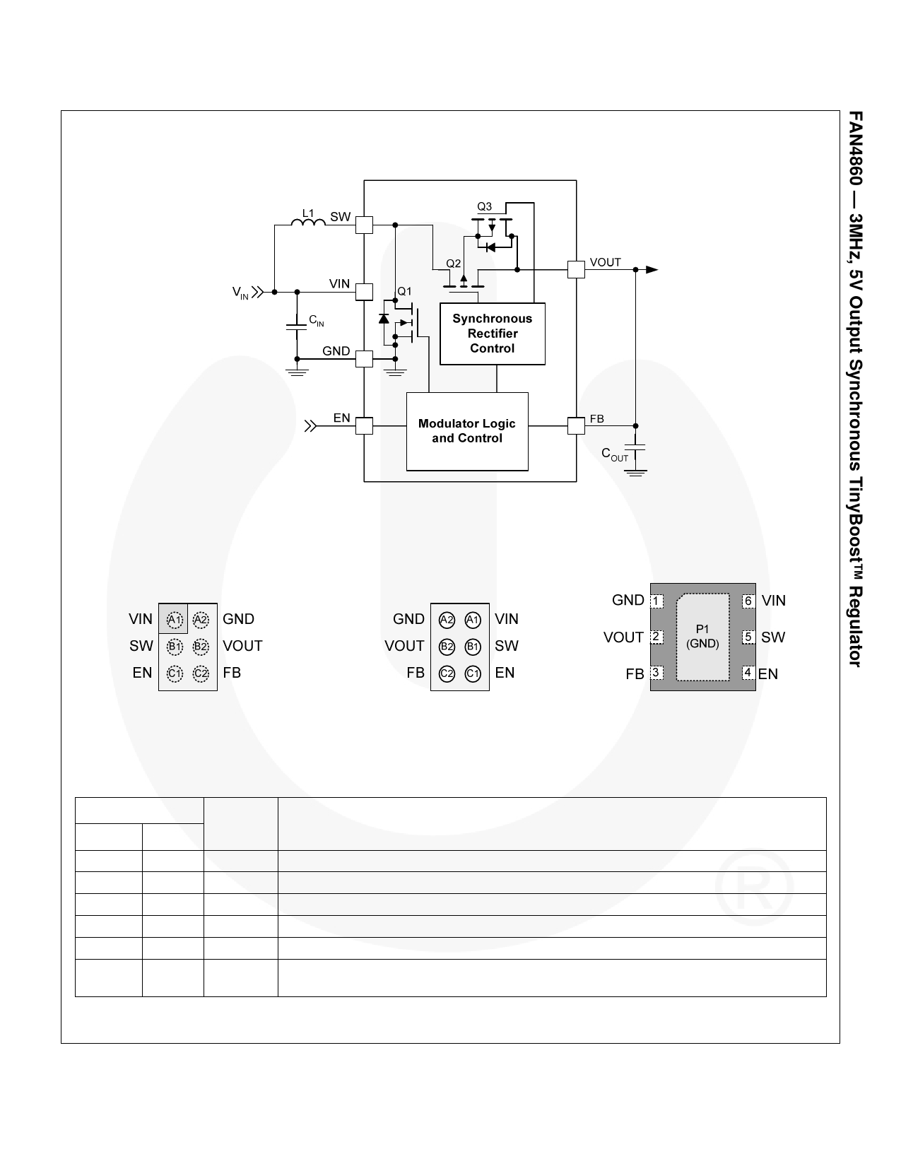
Block Diagrams
Pin Configuration
Figure 2. IC Block Diagram
Figure 3. WLCSP (Top View)
Figure 4. WLCSP (Bottom View)
Figure 5. 2X2mm UMLP (Top View)
Pin Definitions
Pin #
WLCSP UMLP
A1
6
B1
5
C1
4
C2
3
B2
2
A2
1, P1
Name Description
VIN
SW
EN
FB
VOUT
GND
Input Voltage. Connect to Li-Ion battery input power source and input capacitor (CIN).
Switching Node. Connect to inductor.
Enable. When this pin is HIGH, the circuit is enabled. This pin should not be left floating.
Feedback. Output voltage sense point for VOUT. Connect to output capacitor (COUT).
Output Voltage. This pin is both the output voltage terminal as well as an IC bias supply.
Ground. Power and signal ground reference for the IC. All voltages are measured with
respect to this pin.
© 2009 Fairchild Semiconductor Corporation
FAN4860 • Rev. 1.0.3
2
www.fairchildsemi.com
Share Link: 