M50LPW040K データシートの表示(PDF) - STMicroelectronics
部品番号
コンポーネント説明
メーカー
M50LPW040K Datasheet PDF : 36 Pages
| |||
M50LPW040
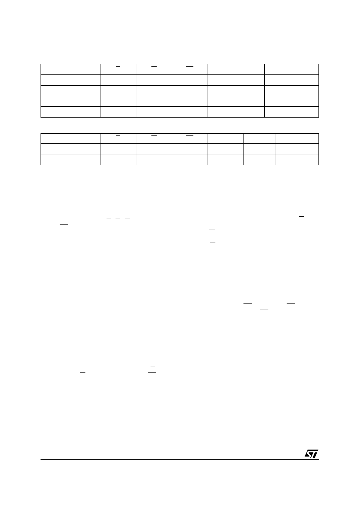
Table 8. A/A Mux Bus Operations
Operation
G
W
RP
Bus Read
VIL
VIH
VIH
Bus Write
VIH
VIL
VIH
Output Disable
VIH
VIH
VIH
Reset
VIL or VIH
VIL or VIH
VIL
Table 9. Manufacturer and Device Codes
Operation
G
W
RP
Manufacturer Code
VIL
VIH
VIH
Device Code
VIL
VIH
VIH
VPP
Don’t Care
VCC or VPPH
Don’t Care
Don’t Care
DQ7-DQ0
Data Output
Data Input
Hi-Z
Hi-Z
A18-A1
A0
DQ7-DQ0
VIL
VIL
20h
VIL
VIH
26h
Address/Address Multiplexed (A/A Mux) Bus
Operations
The Address/Address Multiplexed (A/A Mux)
Interface has a more traditional style interface.
The signals consist of a multiplexed address
signals (A0-A10), data signals, (DQ0-DQ7) and
three control signals (RC, G, W). An additional
signal, RP, can be used to reset the memory.
The Address/Address Multiplexed (A/A Mux)
Interface is included for use by Flash
Programming equipment for faster factory
programming. Only a subset of the features
available to the Low Pin Count (LPC) Interface are
available; these include all the Commands but
exclude the Security features and other registers.
The following operations can be performed using
the appropriate bus cycles: Bus Read, Bus Write,
Output Disable and Reset.
When the Address/Address Multiplexed (A/A Mux)
Interface is selected all the blocks are
unprotected. It is not possible to protect any blocks
through this interface.
Bus Read. Bus Read operations are used to
output the contents of the Memory Array, the
Electronic Signature and the Status Register. A
valid Bus Read operation begins by latching the
Row Address and Column Address signals into
the memory using the Address Inputs, A0-A10,
and the Row/Column Address Select RC. Then
Write Enable (W) and Interface Reset (RP) must
be High, VIH, and Output Enable, G, Low, VIL, in
order to perform a Bus Read operation. The Data
Inputs/Outputs will output the value, see Figure
12, A/A Mux Interface Read AC Waveforms, and
Table 24, A/A Mux Interface Read AC
Characteristics, for details of when the output
becomes valid.
Bus Write. Bus Write operations write to the
Command Interface. A valid Bus Write operation
begins by latching the Row Address and Column
Address signals into the memory using the
Address Inputs, A0-A10, and the Row/Column
Address Select RC. The data should be set up on
the Data Inputs/Outputs; Output Enable, G, and
Interface Reset, RP, must be High, VIH and Write
Enable, W, must be Low, VIL. The Data Inputs/
Outputs are latched on the rising edge of Write
Enable, W. See Figure 13, A/A Mux Interface
Write AC Waveforms, and Table 25, A/A Mux
Interface Write AC Characteristics, for details of
the timing requirements.
Output Disable. The data outputs are high-im-
pedance when the Output Enable, G, is at VIH.
Reset. During Reset mode all internal circuits are
switched off, the memory is deselected and the
outputs are put in high-impedance. The memory is
in Reset mode when RP is Low, VIL. RP must be
held Low, VIL for tPLPH. If RP is goes Low, VIL,
during a Program or Erase operation, the
operation is aborted and the memory cells affected
no longer contain valid data; the memory can take
up to tPLRH to abort a Program or Erase operation.
COMMAND INTERFACE
All Bus Write operations to the memory are
interpreted by the Command Interface.
Commands consist of one or more sequential Bus
Write operations.
After power-up or a Reset operation the memory
enters Read mode.
The commands are summarized in Table 11,
Commands. Refer to Table 11 in conjunction with
the text descriptions below.
10/36
Share Link: 