M50LPW040 データシートの表示(PDF) - STMicroelectronics
部品番号
コンポーネント説明
メーカー
M50LPW040 Datasheet PDF : 36 Pages
| |||
M50LPW040
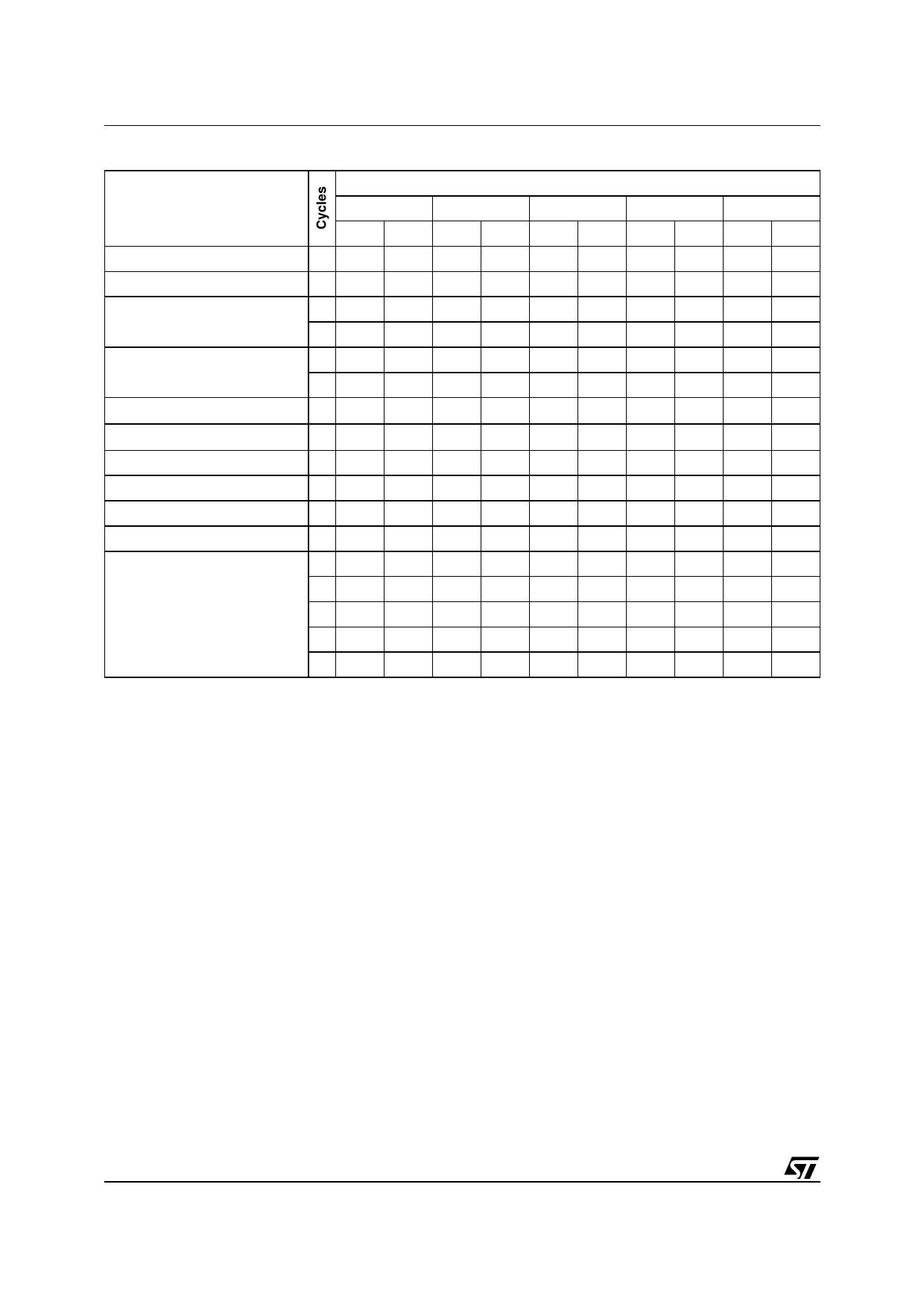
Table 11. Commands
Bus Write Operations
Command
1st
2nd
3rd
4th
5th
Addr Data Addr Data Addr Data Addr Data Addr Data
Read Memory Array
1 X FFh
Read Status Register
1 X 70h
Read Electronic Signature
1 X 90h
1 X 98h
Program
2 X 40h PA PD
2 X 10h PA PD
Quadruple Byte Program
5X
30h A1
PD
A2
PD
A3
PD
A4
PD
Chip Erase
2 X 80h X 10h
Block Erase
2 X 20h BA D0h
Clear Status Register
1 X 50h
Program/Erase Suspend
1 X B0h
Program/Erase Resume
1 X D0h
1 X 00h
1 X 01h
Invalid/Reserved
1 X 60h
1 X 2Fh
1 X C0h
Note: X Don’t Care, PA Program Address, PD Program Data, A1,2,3,4 Consecutive Addresses, BA Any address in the Block.
Read Memory Array. After a Read Memory Array command, read the memory as normal until another command is issued.
Read Status Register. After a Read Status Register command, read the Status Register as normal until another command is issued.
Read Electronic Signature. After a Read Electronic Signature command, read Manufacturer Code, Device Code until a Read Mem-
ory Array command is issued.
Block Erase, Program. After these commands read the Status Register until the command completes and another command is is-
sued.
Quadruple Byte Program. This command is only valid in A/A Mux mode. Addresses A1, A2, A3 and A4 must be consecutive addresses
differing only for address bit A0 and A1. After this command read the Status Register until the command completes and another com-
mand is issued.
Chip Erase. This command is only valid in A/A Mux mode. After this command read the Status Register until the command completes
and another command is issued.
Clear Status Register. After the Clear Status Register command bits 1, 3, 4 and 5 in the Status Register are reset to ‘0’.
Program/Erase Suspend. After the Program/Erase Suspend command has been accepted, issue Read Memory Array, Read Status
Register, Program (during Erase suspend) and Program/Erase resume commands.
Program/Erase Resume. After the Program/Erase Resume command the suspended Program/Erase operation resumes, read the
Status Register until the Program/Erase Controller completes and the memory returns to Read Mode.
Invalid/Reserved. Do not use Invalid or Reserved commands.
Status Register. See the section on the Status
Register for details on the definitions of the Status
Register bits. During the Chip Erase operation the
memory will only accept the Read Status Register
command. All other commands will be ignored.
Typical Chip Erase times are given in Table 12.
The Chip Erase command sets all of the bits in the
memory to ‘1’. See Figure 17, Chip Erase Flow-
chart and Pseudo Code, for a suggested flowchart
on using the Chip Erase command.
Block Erase Command. The Block Erase com-
mand can be used to erase a block. Two Bus Write
operations are required to issue the command; the
second Bus Write cycle latches the block address
in the internal state machine and starts the Pro-
gram/Erase Controller. Once the command is is-
sued subsequent Bus Read operations read the
Status Register. See the section on the Status
Register for details on the definitions of the Status
Register bits.
If the block is protected then the Block Erase
operation will abort, the data in the block will not be
changed and the Status Register will output the
error.
12/36
Share Link: 