M50LPW040K データシートの表示(PDF) - STMicroelectronics
部品番号
コンポーネント説明
メーカー
M50LPW040K Datasheet PDF : 36 Pages
| |||
M50LPW040
Top Block Lock (TBL). The Top Block Lock
input is used to prevent the Top Block (Block 7)
from being changed. When Top Block Lock, TBL,
is set Low, VIL, Program and Block Erase
operations in the Top Block have no effect,
regardless of the state of the Lock Register. When
Top Block Lock, TBL, is set High, VIH, the
protection of the Block is determined by the Lock
Register. The state of Top Block Lock, TBL, does
not affect the protection of the Main Blocks (Blocks
0 to 6).
Top Block Lock, TBL, must be set prior to a Pro-
gram or Block Erase operation is initiated and
must not be changed until the operation completes
or unpredictable results may occur. Care should
be taken to avoid unpredictable behavior by
changing TBL during Program or Erase Suspend.
Write Protect (WP). The Write Protect input is
used to prevent the Main Blocks (Blocks 0 to 6)
from being changed. When Write Protect, WP, is
set Low, VIL, Program and Block Erase operations
in the Main Blocks have no effect, regardless of
the state of the Lock Register. When Write Protect,
WP, is set High, VIH, the protection of the Block is
determined by the Lock Register. The state of
Write Protect, WP, does not affect the protection of
the Top Block (Block 7).
Write Protect, WP, must be set prior to a Program
or Block Erase operation is initiated and must not
be changed until the operation completes or un-
predictable results may occur. Care should be tak-
en to avoid unpredictable behavior by changing
WP during Program or Erase Suspend.
Reserved for Future Use (RFU). These pins do
not have assigned functions in this revision of the
part. They must be left disconnected. (Pin 9 in the
PLCC32, and Pin 21 in the TSOP40, may also be
driven High or driven Low.)
Address/Address Multiplexed (A/A Mux)
Signal Descriptions
For the Address/Address Multiplexed (A/A Mux)
Interface see Figure 2, Logic Diagram, and Table
3, Signal Names.
Address Inputs (A0-A10). The Address Inputs
are used to set the Row Address bits (A0-A10) and
the Column Address bits (A11-A18). They are
latched during any bus operation by the Row/Col-
umn Address Select input, RC.
Data Inputs/Outputs (DQ0-DQ7). The Data In-
puts/Outputs hold the data that is written to or read
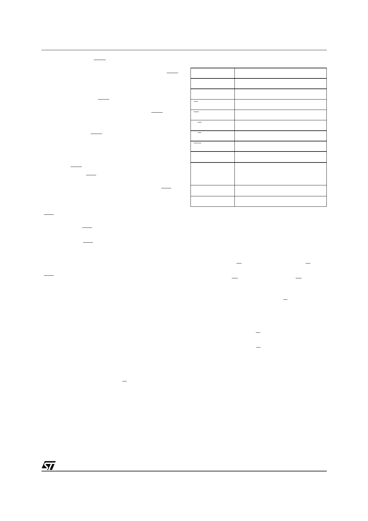
Table 3. Signal Names (A/A Mux Interface)
IC
Interface Configuration
A0-A10
Address Inputs
DQ0-DQ7
Data Inputs/Outputs
G
Output Enable
W
Write Enable
RC
Row/Column Address Select
RB
Ready/Busy Output
RP
Interface Reset
VCC
Supply Voltage
Optional Supply Voltage for Fast
VPP
Program and Fast Erase
Operations
VSS
Ground
NC
Not Connected Internally
from the memory. They output the data stored at
the selected address during a Bus Read opera-
tion. During Bus Write operations they represent
the commands sent to the Command Interface of
the internal state machine. The Data Inputs/Out-
puts, DQ0-DQ7, are latched during a Bus Write
operation.
Output Enable (G). The Output Enable, G, con-
trols the Bus Read operation of the memory.
Write Enable (W). The Write Enable, W, controls
the Bus Write operation of the memory’s Com-
mand Interface.
Row/Column Address Select (RC). The Row/
Column Address Select input selects whether the
Address Inputs should be latched into the Row
Address bits (A0-A10) or the Column Address bits
(A11-A18). The Row Address bits are latched on
the falling edge of RC whereas the Column
Address bits are latched on the rising edge.
Ready/Busy Output (RB). The Ready/Busy pin
gives the status of the memory’s Program/Erase
Controller. When Ready/Busy is Low, VOL, the
memory is busy with a Program or Erase operation
and it will not accept any additional Program or
Erase command except the Program/Erase
Suspend command. When Ready/Busy is High,
VOH, the memory is ready for any Read, Program
or Erase operation.
5/36
Share Link: 