PDM31098SA10SO データシートの表示(PDF) - Paradigm Technology
部品番号
コンポーネント説明
メーカー
PDM31098SA10SO Datasheet PDF : 8 Pages
| |||
PRELIMINARY
PDM31098
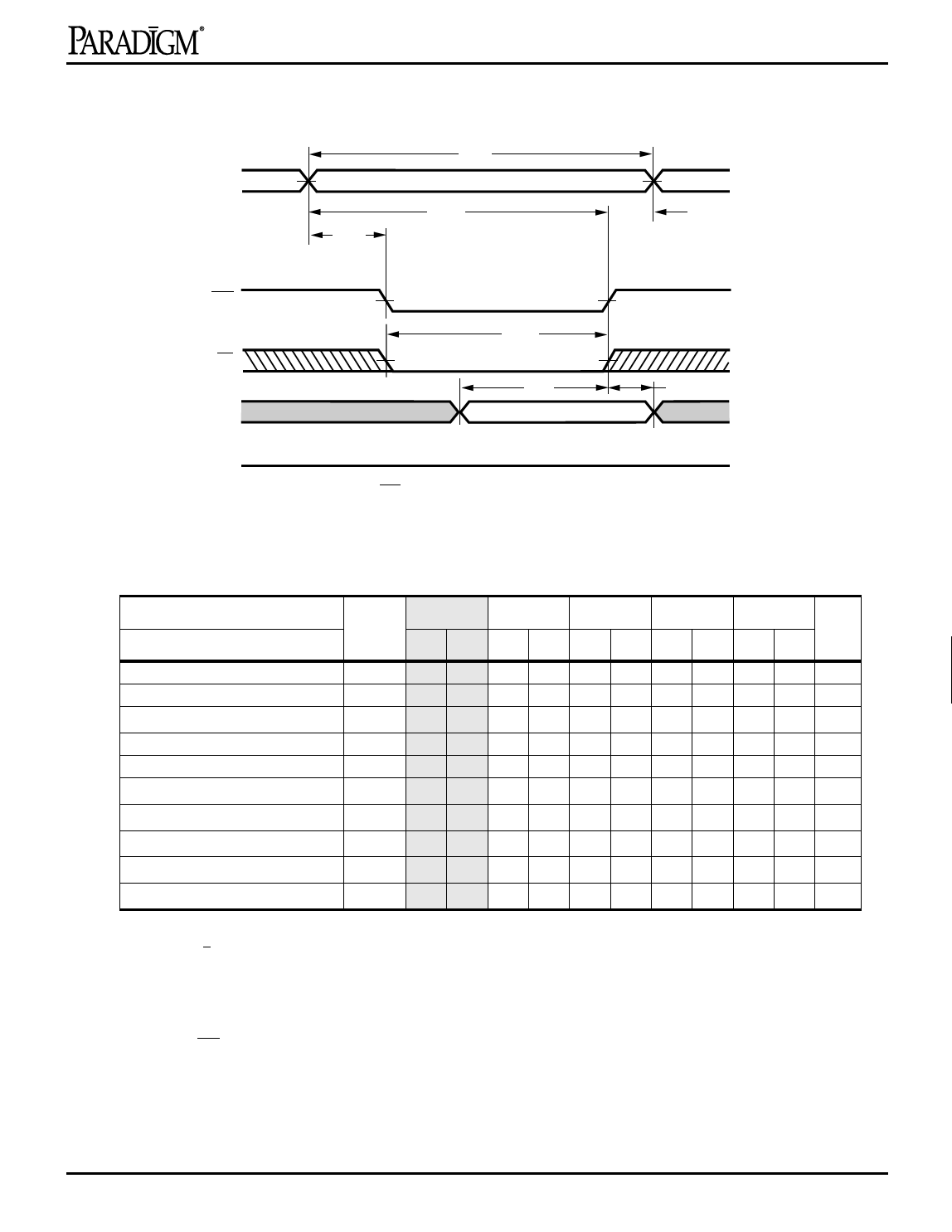
Write Cycle No. 3 (Chip Enable Controlled)
tWC
1
ADDR
tAW
tAH
tAS
2
CE1
tWP1
3
WE
tDS
tDH
DIN
DATA VALID
4
DOUT
HIGH-Z
NOTE: Output Enable (OE) is inactive (high)
5
AC Electrical Characteristics
6
Description
-8*
-10*
-12
-15
-20
WRITE Cycle
WRITE cycle time
Sym Min. Max. Min. Max. Min. Max. Min. Max. Min. Max. Units
tWC
8 — 10 — 12 — 15 — 20 — ns
7
Chip enable to end of write
tCW
7 — 8 — 10 — 11 — 13 — ns
Address valid to end of write
tAW
7 — 8 — 10 — 11 — 13 — ns
Address setup time
Address hold from end of write
tAS
0 — 0 — 0 — 0 — 0 — ns
tAH
0 — 0 — 0 — 0 — 0 — ns
8
Write pulse width
tWP
7 — 8 — 8 — 9 — 10 — ns
Data setup time
Data hold time
tDS
5 — 6 — 7 — 8 — 9 — ns
tDH
0 — 0 — 0 — 0 — 0 — ns
9
Write disable to output in low Z(1,3)
tLZWE
0
—
0
—
0
—
0—
0
— ns
Write enable to output in high Z(1,3) tHZWE —
4
—
5
—6
—
7
—
9
ns
SHADED AREA = PRELIMINARY DATA
10
* VCC = 3.3V + 5%
NOTES: (For two previous Electrical Characteristics tables)
1.The parameter is tested with CL = 5 pF as shown in Figure 2. Transition is measured ±200 mV from steady state
voltage.
2.At any given temperature and voltage condition, tHZCE is less than tLZCE.
3.This parameter is sampled.
11
4.WE is high for a READ cycle.
5.The device is continuously selected. All the Chip Enables are held in their active state.
6.The address is valid prior to or coincident with the latest occuring Chip Enable.
12
Rev. 1.3 - 5/27/98
7
Share Link: 