QL3004E データシートの表示(PDF) - QuickLogic Corporation
部品番号
コンポーネント説明
メーカー
QL3004E
QuickLogic Corporation

QL3004E Datasheet PDF : 49 Pages
| |||
pASIC 3 FPGA Family Data Sheet Rev. D
Electrical Specifications
AC Characteristics at VCC = 3.3 V, TA = 25°C (K = 1.00)
To calculate delays, multiply the appropriate K factor from Table 9 by the numbers provided in Table 3
through Table 7.
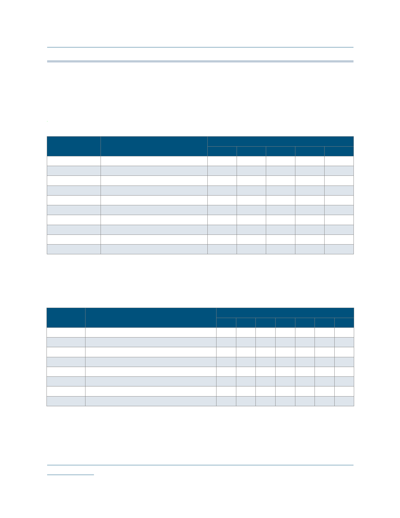
Table 3: Logic Cells
Symbol
tPD
tSU
tH
tCLK
tCWHI
tCWLO
tSET
tRESET
tSW
tRW
Parameter
Combinatorial Delay b
Setup Time b
Hold Time
Clock to Q Delay
Clock High Time
Clock Low Time
Set Delay
Reset Delay
Set Width
Reset Width
Propagation Delays (ns) Fanouta
1
2
3
4
8
1.4
1.7
1.9
2.2
3.2
1.7
1.7
1.7
1.7
1.7
0.0
0.0
0.0
0.0
0.0
0.7
1.0
1.2
1.5
2.5
1.2
1.2
1.2
1.2
1.2
1.2
1.2
1.2
1.2
1.2
1.0
1.3
1.5
1.8
2.8
0.8
1.1
1.3
1.6
2.6
1.9
1.9
1.9
1.9
1.9
1.8
1.8
1.8
1.8
1.8
a. Stated timing for worst case Propagation Delay over process variation at VCC = 3.3 V and TA = 25°C. Multiply by the appropriate
Delay Factor, K, for speed grade, voltage, and temperature settings as specified in Table 9.
b. These limits are derived from a representative selection of the slowest paths through the pASIC 3 logic cell including typical net
delays. Worst case delay values for specific paths should be determined from timing analysis of your particular design.
Table 4: Input-Only/Clock Cells
Symbol
Parameter
Propagation Delays (ns) Fanout a
1
2
3
4
8 12 24
tIN
High Drive Input Delay
1.5 1.6 1.8 1.9 2.4 2.9 4.4
tINI
High Drive Input, Inverting Delay
1.6 1.7 1.9 2.0 2.5 3.0 4.5
tISU
Input Register Set-Up Time
3.1 3.1 3.1 3.1 3.1 3.1 3.1
tIH
Input Register Hold Time
0.0 0.0 0.0 0.0 0.0 0.0 0.0
tlCLK
Input Register Clock To Q
0.7 0.8 1.0 1.1 1.6 2.1 3.6
tlRST
Input Register Reset Delay
0.6 0.7 0.9 1.0 1.5 2.0 3.5
tlESU
Input Register clock Enable Set-Up Time
2.3 2.3 2.3 2.3 2.3 2.3 2.3
tlEH
Input Register Clock Enable Hold Time
0.0 0.0 0.0 0.0 0.0 0.0 0.0
a. Stated timing for worst case Propagation Delay over process variation at VCC = 3.3 V and TA = 25°C. Multiply by the appropriate
Delay Factor, K, for speed grade, voltage, and temperature settings as specified in Table 9.
4
•
•••
••
www.quicklogic.com
© 2005 QuickLogic Corporation
Share Link: