AD694 データシートの表示(PDF) - Analog Devices
部品番号
コンポーネント説明
メーカー
AD694 Datasheet PDF : 16 Pages
| |||
AD694
optional NPN pass transistor can be added to transfer most of
the power dissipation off-chip, to extend the temperature range
of operation.
The output stage is current-limited at approximately 38 mA to
protect the output from an overdrive at its inputs. The V/I will
allow linear operation to approximately 24 mA. The V/I con-
verter also has an open collector alarm (Pin 10) which warns of
open-circuit condition at the IOUT pin or of attempts to drive the
output to a voltage greater than VS – 2 V.
4 mA OFFSET GENERATOR
This circuit converts a constant voltage from the voltage
reference to a constant current of approximately 200 µA. This
current is summed with the signal current at Pin 14 (BW
Adjust), to result in a constant 4 mA offset current at IOUT. The
4 mA Adj (Pin 6) allows the offset current to be adjusted to any
current in the range of 2 mA to 4.8 mA. Pin 9 (4 mA On/Off)
can shut off the offset current completely if it is lifted to 3.0 V or
more, allowing 0 to 20 mA operation of the AD694. In normal
4–20 mA operation, Pin 9 is connected to ground.
VOLTAGE REFERENCE
A 2 V or 10 V voltage reference is available for user applications,
selectable by pin-strapping. The 10 V option is available for
supply voltages greater than 12.5 V, the 2 V output is available
over the whole 4.5 V to 36 V power supply range. The reference
can source up to 5 mA for user applications. A boost transistor
can be added to increase the current drive capability of the 2 V
mode.
APPLYING THE AD694
The AD694 can easily be connected for either dual or single
supply operation, to operate from supplies as low as 4.5 V and
as high as 36 V. The following sections describe the different
connection configurations, as well as adjustment methods.
Table I shows possible connection options.
Table I. Precalibrated Ranges for the AD694
Input Output Voltage Min
Range Range Reference VS
Pin 9 Pin 4 Pin 8
0–2 V 4–20 mA 2 V
0–10 V 4–20 mA 2 V
0–2.5 V 0–20 mA 2 V
0–12.5 V 0–20 mA 2 V
0–2 V 4–20 mA 10 V
0–10 V 4–20 mA 10 V
0–2.5 V 0–20 mA 10 V
0–12.5 V 0–20 mA 10 V
4.5 V
12.5 V
5.0 V
15.0 V
12.5 V
12.5 V
12.5 V
15.0 V
Pin 5
Pin 5
≥3 V
≥3 V
Pin 5
Pin 5
≥3 V
≥3 V
Pin 5
Open
Pin 5
Open
Pin 5
Open
Pin 5
Open
Pin 7
Pin 7
Pin 7
Pin 7
Open
Open
Open
Open
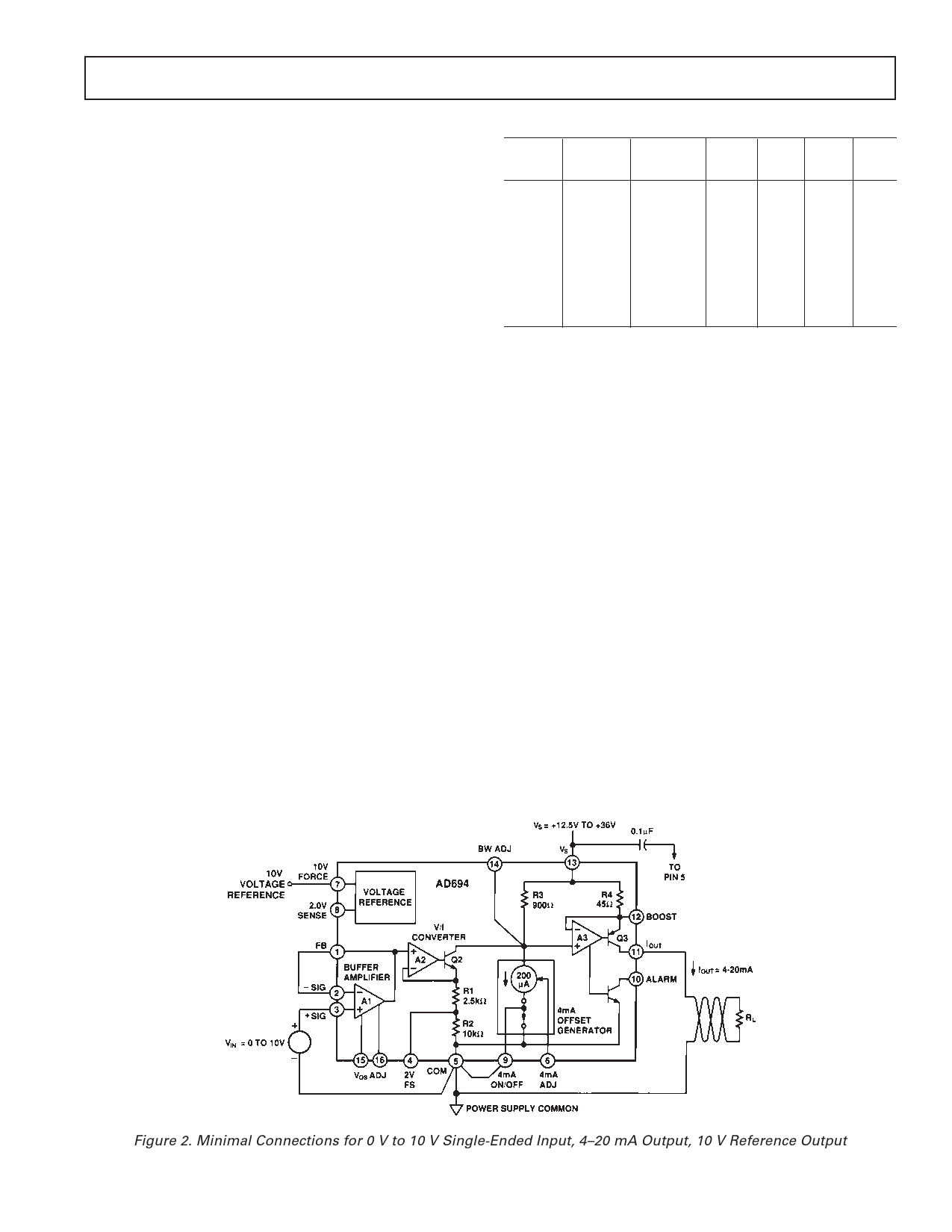
BASIC CONNECTIONS: 12.5 V SINGLE-SUPPLY
OPERATION WITH 10 V FS
Figure 2 shows the minimal connections required for basic
operation with a 12.5 V power supply, 10 V input span,
4–20 mA output span, and a 10 V voltage reference. The buffer
amplifier is connected as a voltage follower to drive the V/I
converter by connecting FB (Pin 1) to –Sig (Pin 2). 4 mA On/
Off (Pin 9) is tied to ground (Pin 5) to enable the 4 mA offset
current. The AD694 can drive a maximum load RL = [VS – 2 V]
/20 mA, thus the maximum load with a 12.5 V supply is 525 Ω.
SELECTING A 2 V FULL-SCALE INPUT
The 2 V full-scale option is selected by shorting Pin 4 (2 V FS)
to Pin 5 (Common). The connection should be as short as pos-
sible; any parasitic resistance will affect the precalibrated span
accuracy.
SELECTING THE 2 V VOLTAGE REFERENCE
The voltage reference is set to a 2 V output by shorting Pin 7 to
Pin 8 (10 V Force to 2 V Sense). If desired, the 2 V reference
can be set up for remote force and sense connection. Keep in
mind that the 2 V Sense line carries a constant current of 100 µA
that could cause an offset error over long wire runs. The 2 V
reference option can be used with all supply voltages greater
than 4.5 V.
Figure 2. Minimal Connections for 0 V to 10 V Single-Ended Input, 4–20 mA Output, 10 V Reference Output
REV. B
–5–
Share Link: 