FM25V01 データシートの表示(PDF) - Cypress Semiconductor
部品番号
コンポーネント説明
メーカー
FM25V01 Datasheet PDF : 18 Pages
| |||
Endurance
The FM25V01 device is capable of being accessed at
least 1014 times, reads or writes. An F-RAM memory
operates with a read and restore mechanism.
Therefore, an endurance cycle is applied on a row
basis for each access (read or write) to the memory
array. The F-RAM architecture is based on an array
of rows and columns. Rows are defined by A13-A3
and column addresses by A2-A0. See Block
Diagram (pg 2) which shows the array as 2K rows of
FM25V01 - 128Kb SPI FRAM
64-bits each. The entire row is internally accessed
once whether a single byte or all eight bytes are read
or written. Each byte in the row is counted only once
in an endurance calculation. The table below shows
endurance calculations for 64-byte repeating loop,
which includes an op-code, a starting address, and a
sequential 64-byte data stream. This causes each byte
to experience one endurance cycle through the loop.
F-RAM read and write endurance is virtually
unlimited even at 40MHz clock rate.
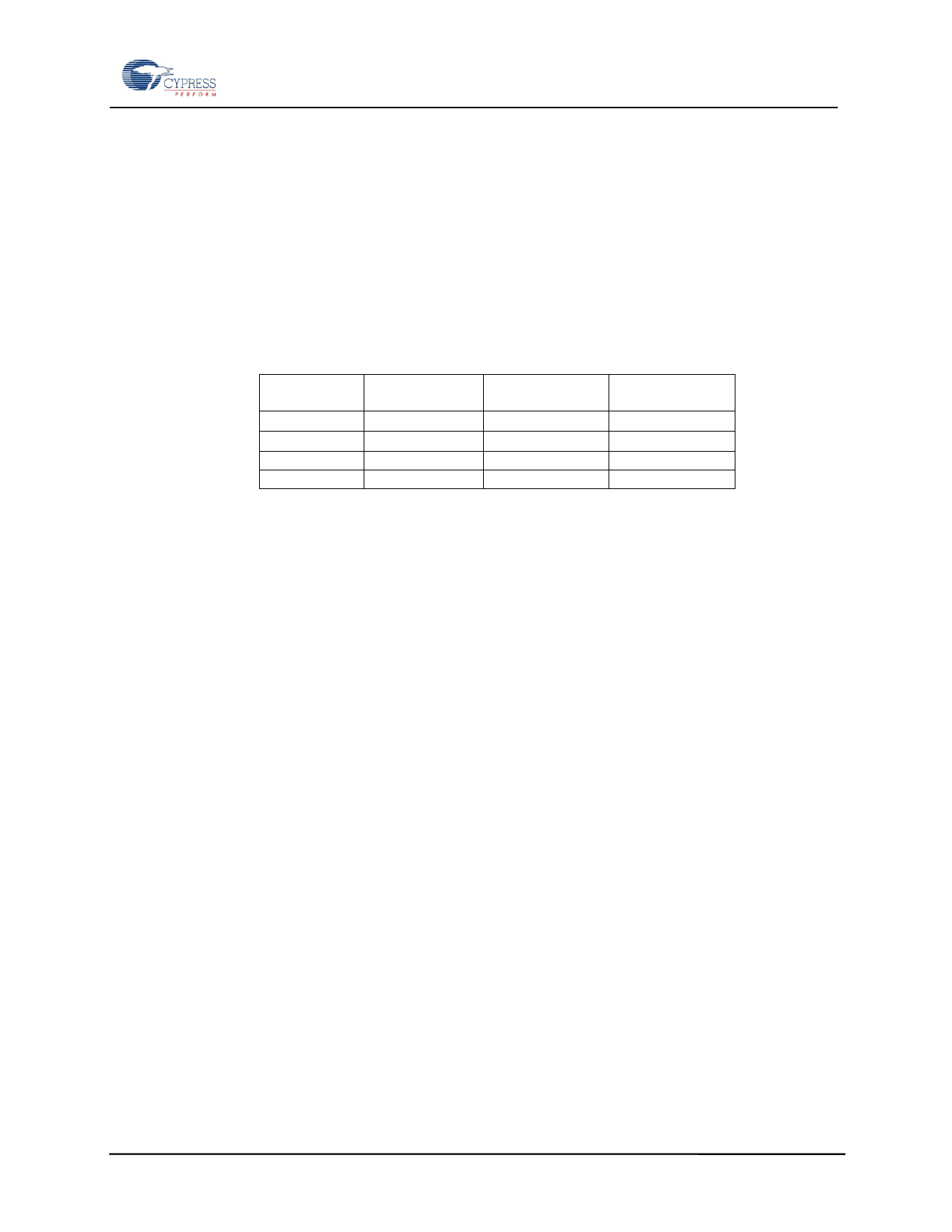
Table 7. Time to Reach 100 Trillion Cycles for Repeating 64-byte Loop
SCK Freq
(MHz)
Endurance
Cycles/sec.
Endurance
Cycles/year
Years to Reach
1014 Cycles
40
74,620
2.35 x 10¹²
42.6
20
37,310
1.18 x 10¹²
85.1
10
18,660
5.88 x 10¹¹
170.2
5
9,330
2.94 x 10¹¹
340.3
Document Number: 001-84492 Rev. *B
Page 10 of 18
Share Link: 