SN74LS77D データシートの表示(PDF) - Motorola => Freescale
部品番号
コンポーネント説明
メーカー
SN74LS77D Datasheet PDF : 4 Pages
| |||
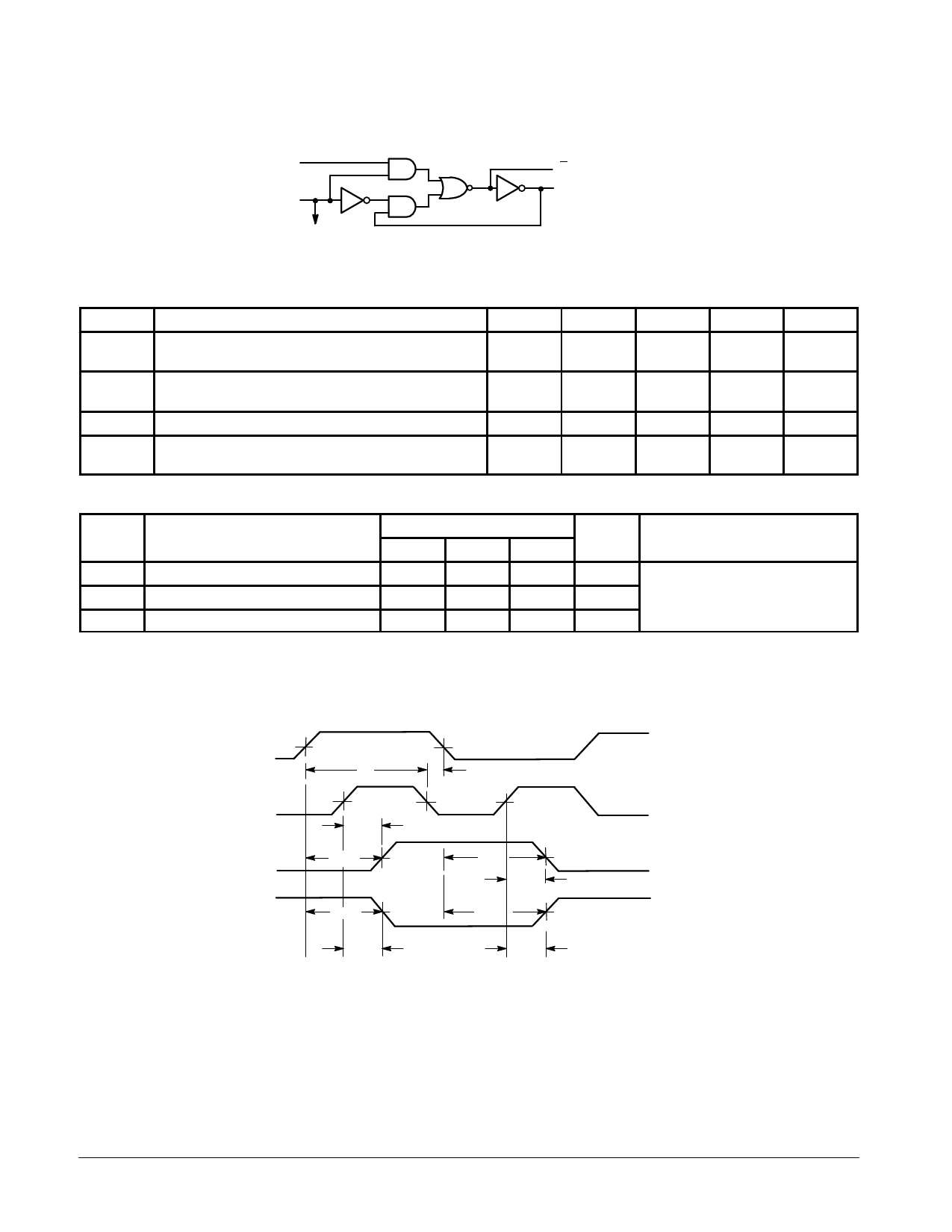
SN54/74LS75 D SN54/74LS77
DATA
ENABLE
TO OTHER LATCH
LOGIC DIAGRAM
Q (SN54/74LS75 ONLY)
Q
GUARANTEED OPERATING RANGES
Symbol
Parameter
VCC
Supply Voltage
TA
Operating Ambient Temperature Range
IOH
Output Current — High
IOL
Output Current — Low
AC SETUP REQUIREMENTS (TA = 25°C, VCC = 5.0 V)
Symbol
Parameter
Min
tW
Enable Pulse Width High
20
ts
Setup Time
20
th
Hold Time
0
Min
54
4.5
74
4.75
54
– 55
74
0
54, 74
54
74
Limits
Typ
Max
Unit
ns
ns
ns
Typ
Max
Unit
5.0
5.5
V
5.0
5.25
25
125
°C
25
70
– 0.4
mA
4.0
mA
8.0
Test Conditions
VCC = 5.0 V
AC WAVEFORMS
D
1.3 V
1.3 V
ts
th
E
1.3 V
1.3 V
1.3 V
tPLH
Q
tPLH
1.3 V
Q
tPHL
1.3 V
tPHL
1.3 V
tPHL
tPLH
1.3 V
tPHL
tPLH
DEFINITION OF TERMS
SETUP TIME (ts) — is defined as the minimum time required for the correct logic level to be present at the logic input prior to the
clock transition from HIGH-to-LOW in order to be recognized and transferred to the outputs.
HOLD TIME (th) — is defined as the minimum time following the clock transition from HIGH-to-LOW that the logic level must be
maintained at the input in order to ensure continued recognition. A negative HOLD TIME indicates that the correct logic level may
be released prior to the clock transition from HIGH-to-LOW and still be recognized.
FAST AND LS TTL DATA
5-4
Share Link: 