SK100E445(2001) データシートの表示(PDF) - Semtech Corporation
部品番号
コンポーネント説明
メーカー
SK100E445 Datasheet PDF : 8 Pages
| |||
HIGH-PER.ORMANCE PRODUCTS
Description
SK10/100E445
4-Bit Serial/Parallel Converter
.eatures
The SK10/100E445 is an integrated 4-bit serial-to-
parallel data converter. The device is designed to operate • On-Chip Clock ÷ 4 and ÷8
for NRZ data rates of up to 2.0 Gb/s. The chip generates • 2.0 Gb/s Data Rate Capability
a divide by 4 and a divide by 8 clock for both 4-bit • Differential Clock and Serial Inputs
conversion and a two chip 8-bit conversion function. The • VBB Output for Single-Ended Input Applications
conversion sequence was chosen to convert the first • Asynchronous Data Synchronization
serial bit to Q0, the second to Q1, etc.
• Mode Select to Expand to 8-Bits
• Internal 75 kΩ Input Pulldown Resistors
Two selectable serial inputs provide a loopback capability • ESD Protection of >4000V
for testing purposes when the device is used in • Extended 100E VEE Range of –4.2V to –5.46V
conjunction with the R446 parallel to serial converter. • Fully Compatible with MC10/100E445
• Available in 28-Pin PLCC Package
The start bit for conversion can be moved using the SYNC
input. A single pulse applied asynchronously for at least
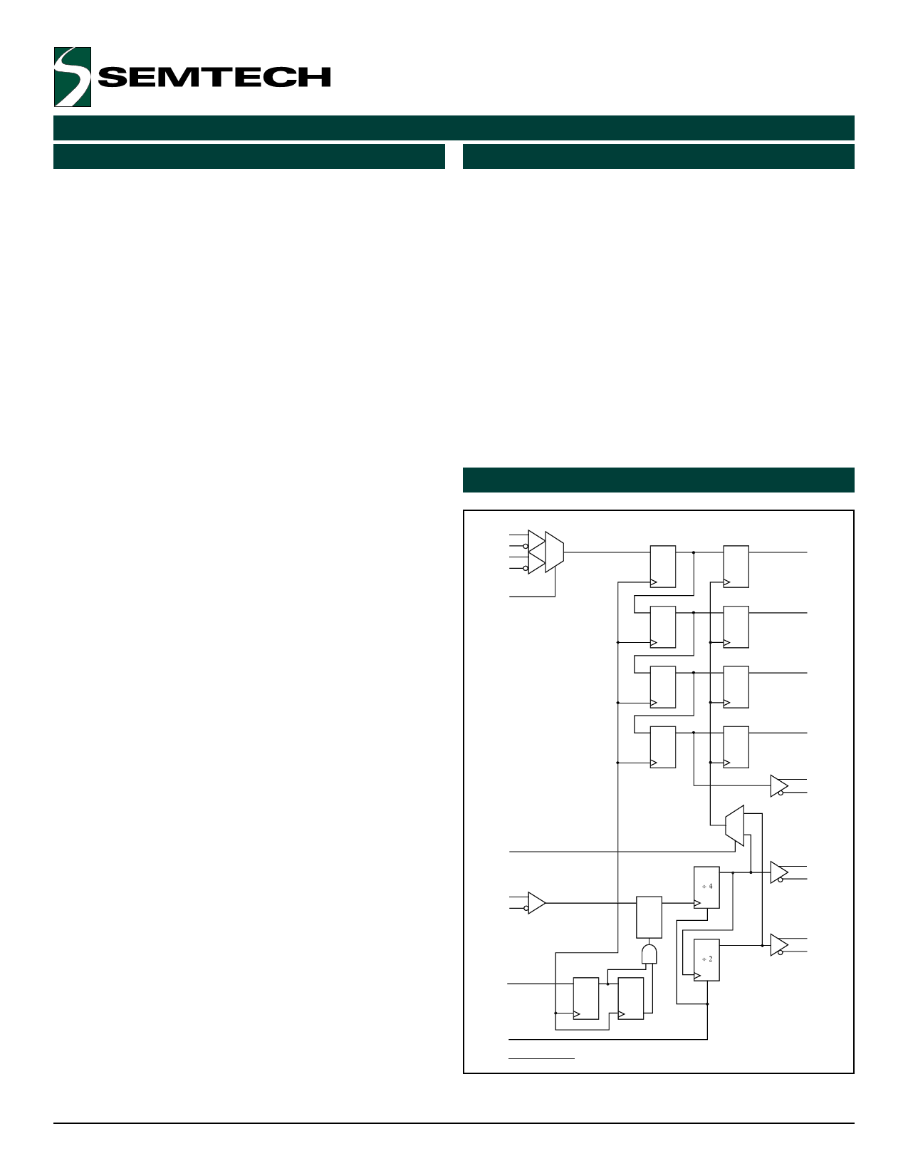
two input clock cycles shifts the start bit for conversion .unctional Block Diagram
from Qn to Qn–1. For each additional shift required, an
additional pulse must be applied to the SYNC input.
Asserting the SYNC input will force the internal clock
SINB
SINB*
dividers to “swallow” a clock pulse, effectively shifting a
SINA
bit from the Qn to the Qn–1 output (see Timing Diagram
SINA*
DQ
DQ
Q3
B).
SEL
The MODE input is used to select the conversion mode
DQ
DQ
Q2
of the device. With the MODE input LOW, or open, the
device will function as a 4-bit converter. When the mode
input is driven HIGH, the data on the output will change
DQ
DQ
Q1
on every eighth clock cycle, thus allowing for an 8-bit
conversion scheme using two E445’s. When cascaded
in an 8-bit conversion scheme, the devices will not
DQ
DQ
Q0
operate at the 2.0 Gb/s data rate of a single device.
Refer to the applications section of this data sheet for
more information on cascading the E445.
SOUT
SOUT*
0
For lower data rate applications, a VBB reference voltage
is supplied for single-ended inputs. When operating at MODE
clock rates above 500 MHz, differential input signals
are recommended. For single-ended inputs, the VBB pin
CLK
is tied to the inverting differential input and bypassed
CLK*
In Out
Latch
1
Out
¸4
R
CL/4
CL/4*
via a 0.01 µF capacitor. The VBB provides the switching
reference for the input differential amplifier. The VBB
EN
Out
¸2
CL/8
CL/8*
can also be used to AC couple an input signal.
R
SYNC
DQ
D
Upon power-up, the internal flip-flops will attain a random
Q*
state. To synchronize multiple E445’s in a system, the
RESET
master reset must be asserted.
Revision 1/.ebruary 21, 2001
1
www.semtech.com
Share Link: 