FSA1156(2004) データシートの表示(PDF) - Fairchild Semiconductor
部品番号
コンポーネント説明
メーカー
FSA1156 Datasheet PDF : 11 Pages
| |||
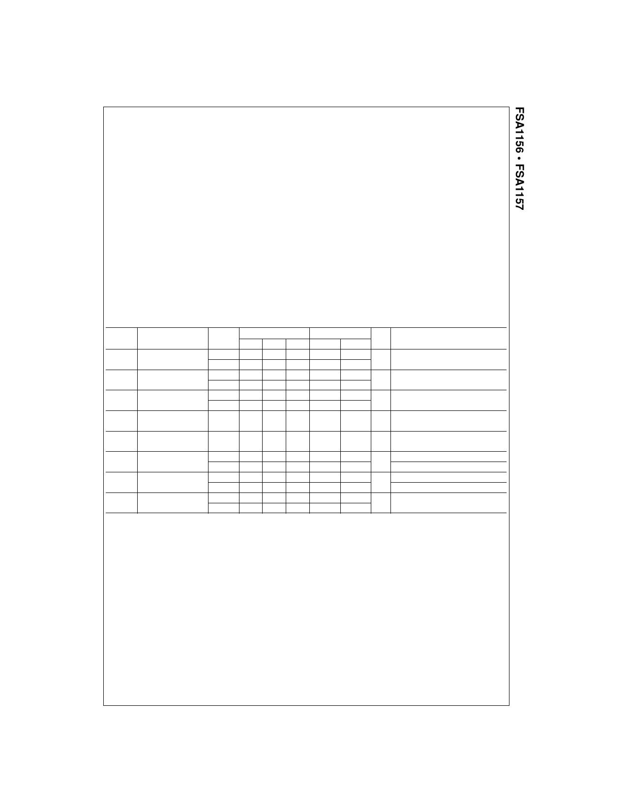
Absolute Maximum Ratings(Note 1)
Supply Voltage (VCC)
Switch Voltage (Note 2)
Input Voltage (VIN) (Note 2)
Input Diode Current
Switch Current
Peak Switch Current
(Pulsed at 1mS duration,
<10% Duty Cycle)
Power Dissipation at 85°C
SC70 package
Storage Temperature Range (TSTG)
Maximum Junction Temperature (TJ)
Lead Temperature (TL)
(Soldering, 10 seconds)
ESD (Human Body Model)
−0.5V to +6.0V
−0.5V to VCC +0.5V
−0.5V to +6.0V
−50 mA
200 mA
400 mA
180 mW
−60°C to +150°C
+150°C
+260°C
8000V
Recommended Operating
Conditions (Note 3)
Supply Voltage (VCC)
Control Input Voltage (Note 3)
Switch Input Voltage
Operating Temperature
Thermal Resistance θJA in Still Air
SC70 package
1.65V to 5.5V
0V to VCC
0V to VCC
−40°C to 85°C
350°C/W
Note 1: The “Absolute Maximum Ratings” are those values beyond which
the safety of the device cannot be guaranteed. The device should not be
operated at these limits. The parametric values defined in the Electrical
Characteristics tables are not guaranteed at the absolute maximum rating.
The “Recommended Operating Conditions” table will define the conditions
for actual device operation.
Note 2: The input and output negative ratings may be exceeded if the input
and output diode current ratings are observed.
Note 3: Control input must be held HIGH or LOW and it must not float.
DC Electrical Characteristics (all typical values are at 25°C unless otherwise specified)
Symbol
Parameter
VCC
TA = +25 °C
TA = −40°C to +85°C Units
(V)
Min Typ Max Min
Max
Conditions
VIH
Input Voltage HIGH
2.7 to 3.6
4.5 to 5.5
2.0
V
2.4
VIL
Input Voltage LOW
2.7 to 3.6
4.5 to 5.5
0.6
V
0.8
IIN
Control Input Leakage 2.7 to 3.6
4.5 to 5.5
−1.0
−1.0
1.0
1.0
µA VIN = 0V to VCC
INO(OFF),
INC(OFF)
IA(ON)
OFF Leakage
Current
ON Leakage
Current
5.5
−2.0
5.5
−4.0
2.0 −20.0
4.0 −40.0
A = 1V, 4.5V
20.0 nA
B = 4.5V, 1V
A = 1V, 4.5V
40.0 nA
B = 1V, 4.5V or Floating
RON
Switch On Resistance
2.7
(Note 4)
4.5
RFLAT(ON) On Resistance Flatness
2.7
(Note 5)
4.5
ICC
Quiescent Supply
3.6
Current
5.5
1.4 2.1
0.75 0.9
0.6
0.1 0.2
0.1 0.5
0.1 0.5
2.5
Ω IOUT = 100mA, B = 1.5V
1.0
IOUT = 100mA, B = 3.5V
Ω IOUT = 100mA, B0 = 0V, 0.75V,1.5V
0.3
IOUT = 100mA, B0 = 0V, 1V, 2V
1.0
1.0
µA VIN = 0V or VCC, IOUT = 0V
Note 4: On Resistance is determined by the voltage drop between A and B pins at the indicated current through the switch.
Note 5: Flatness is defined as the difference between the maximum and minimum value of On Resistance over the specified range of conditions.
3
www.fairchildsemi.com
Share Link: 