FSDM0465RB データシートの表示(PDF) - Fairchild Semiconductor
部品番号
コンポーネント説明
メーカー
FSDM0465RB Datasheet PDF : 18 Pages
| |||
FSDM0465RB
Functional Description
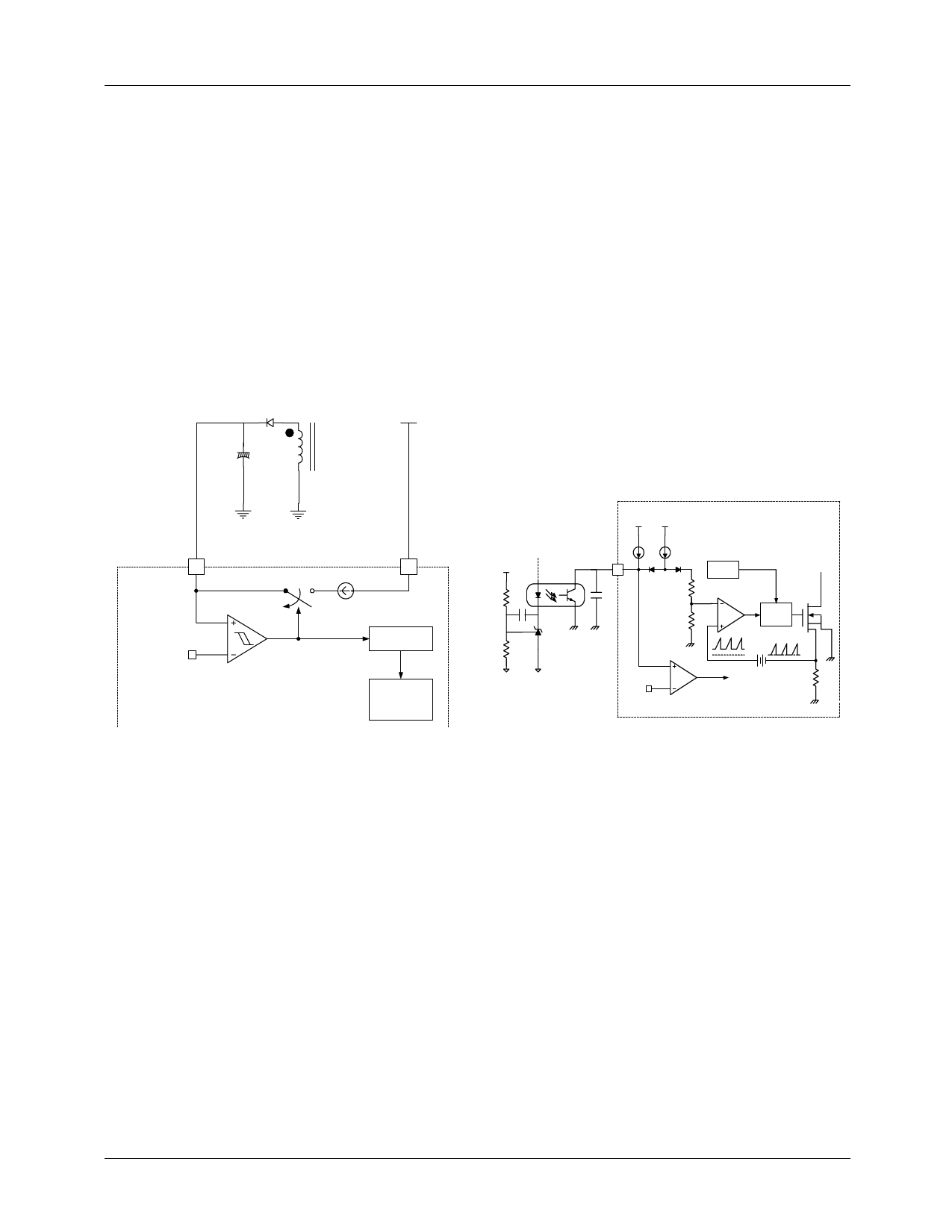
1. Startup: In previous generations of Fairchild Power
Switches (FPSTM) the Vcc pin had an external start-up
resistor to the DC input voltage line. In this generation the
startup resistor is replaced by an internal high voltage current
source. At startup, an internal high voltage current source
supplies the internal bias and charges the external capacitor
(Ca) that is connected to the Vcc pin as illustrated in Figure
4. When Vcc reaches 12V, the FSDM0465RB begins
switching and the internal high voltage current source is
disabled. Then, the FSDM0465RB continues its normal
switching operation and the power is supplied from the
auxiliary transformer winding unless Vcc goes below the
stop voltage of 8V.
VDC
Ca
2.1 Pulse-by-Pulse Current Limit: Because current mode
control is employed, the peak current through the SenseFET
is limited by the inverting input of the PWM comparator
(Vfb*) as shown in Figure 5. Assuming that the 0.9mA
current source flows only through the internal resistor (2.5R
+R= 2.8 kΩ), the cathode voltage of diode D2 is about 2.5V.
Since D1 is blocked when the feedback voltage (Vfb)
exceeds 2.5V, the maximum voltage of the cathode of D2 is
clamped at this voltage, thus clamping Vfb*. Therefore, the
peak value of the current through the SenseFET is limited.
2.2 Leading Edge Blanking (LEB): At the instant the
internal SenseFET is turned on, there usually exists a high
current spike through the SenseFET, caused by primary-side
capacitance and secondary-side rectifier reverse recovery.
Excessive voltage across the Rsense resistor would lead to
incorrect feedback operation in the current mode PWM
control. To counter this effect, the FSDM0465RB employs
an LEB circuit. This circuit inhibits the PWM comparator for
a short time (TLEB) after the, SenseFET is turned on.
Vcc
3
8V/12V
VVccccGgoooodd
6 Vstr
ICH
Vref
Internal
Bias
Vcc Vref
Idelay
IFB
Vo
Vfb
4
H11A817A
CB
OSC
D1 D2
2.5R
KA431
+
Vfb* R
-
SenseFET
GGaattee
Ddriivveer r
VSD
OLP
Rsense
Figure 4. Internal Startup Circuit
2. Feedback Control: FSDM0465RB employs current
mode control, as shown in Figure 5. An opto-coupler (such
as the H11A817A) and shunt regulator (such as the KA431)
are typically used to implement the feedback network.
Comparing the feedback voltage with the voltage across the
Rsense resistor plus an offset voltage makes it possible to
control the switching duty cycle. When the reference pin
voltage of the KA431 exceeds the internal reference voltage
of 2.5V, the H11A817A LED current increases, thus
decreasing the feedback voltage and reducing the duty cycle.
This event typically happens when the input voltage is
increased or the output load is decreased.
Figure 5. Pulse Width Modulation (PWM) Circuit
3. Protection Circuit: The FSDM0465RB has several self
protective functions such as over load protection (OLP), over
voltage protection (OVP), and thermal shutdown (TSD).
Because these protection circuits are fully integrated into the
IC without external components, the reliability can be
improved without increasing cost. Once the fault condition
occurs, switching is terminated and the SenseFET remains
off. This causes Vcc to fall. When Vcc reaches the UVLO
stop voltage, 8V, the protection is reset and the internal high
voltage current source charges the Vcc capacitor via the Vstr
pin. When Vcc reaches the UVLO start voltage,12V, the
FSDM0465RB resumes its normal operation. In this manner,
the auto-restart can alternately enable and disable the
switching of the power Sense FET until the fault condition is
eliminated (see Figure 6).
10
Share Link: 