FTF3020-M データシートの表示(PDF) - Philips Electronics
部品番号
コンポーネント説明
メーカー
FTF3020-M Datasheet PDF : 16 Pages
| |||
Philips Semiconductors
Full Frame CCD Image Sensor
Product specification
FTF3020-M
Specifications
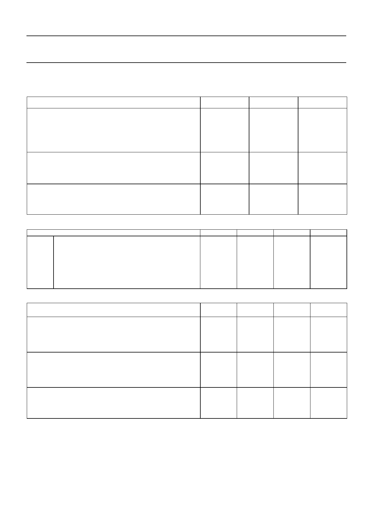
ABSOLUTE MAXIMUM RATINGS1
GENERAL:
storage temperature
ambient temperature during operation
voltage between any two gates
DC current through any clock phase (absolute value)
OUT current (no short circuit protection)
VOLTAGES IN RELATION TO VPS:
VNS, SFD, RD
VCS, SFS
all other pins
VOLTAGES IN RELATION TO VNS:
SFD, RD
VCS, SFS, VPS
all other pins
VNS3
VPS
SFD
SFS
VCS
OG
RD
DC CONDITIONS2
N substrate
P substrate
Source Follower Drain
Source Follower Source
Current Source
Output Gate
Reset Drain
MIN.
-55
-40
-20
-0.2
0
-0.5
-8
-5
-15
-30
-30
MAX.
+80
+60
+20
+2.0
10
+30
+5
+25
+0.5
+0.5
+0.5
UNIT
°C
°C
V
µA
mA
V
V
V
V
V
V
MIN. [V]
18
1
16
0
-5
4
13
TYPICAL [V] MAX. [V]
24
28
3
7
20
24
0
0
0
3
6.5
8
15.5
18
MAX. [mA]
15
15
4.5
1
-
-
-
AC CLOCK LEVEL CONDITIONS2
IMAGE CLOCKS:
A-clock amplitude during integration and hold
A-clock amplitude during vertical transport (duty cycle=5/8) 4
A-clock low level
Charge Reset (CR) level on A-clock 5
OUTPUT REGISTER CLOCKS:
C-clock amplitude (duty cycle during hor. transport = 3/6)
C-clock low level
Summing Gate (SG) amplitude
Summing Gate (SG) low level
OTHER CLOCKS:
Reset Gate (RG) amplitude
Reset Gate (RG) low level
Charge Reset (CR) pulse on Nsub 5
MIN.
8
10
-5
4.75
2
5
0
TYPICAL
MAX.
UNIT
10
V
14
V
0
V
-5
V
5
5.25
V
3.5
V
10
10
V
3.5
V
10
10
V
3
V
10
10
V
1 During Charge Reset it is allowed to exceed maximum rating levels (see note 5).
2 All voltages in relation to SFS.
3 To set the VNS voltage for optimal Vertical Anti-Blooming (VAB), it should be adjustable between minimum and maximum values.
4 Three-level clock is preferred for maximum charge; the swing during vertical transport should be 4V higher than the voltage during integration.
A two level clock (typically 10V) can be used if a lower maximum charge handling capacity is allowed.
5 Charge Reset can be achieved in two ways:
• The typical A-clock low level is applied to all image clocks; for proper CR, an additional Charge Reset pulse on VNS is required (preferred).
• The typical CR level is applied to all image clocks simultaneously.
1999 November
5
Share Link: 