FTF3020-M データシートの表示(PDF) - Philips Electronics
部品番号
コンポーネント説明
メーカー
FTF3020-M Datasheet PDF : 16 Pages
| |||
Philips Semiconductors
Full Frame CCD Image Sensor
Product specification
FTF3020-M
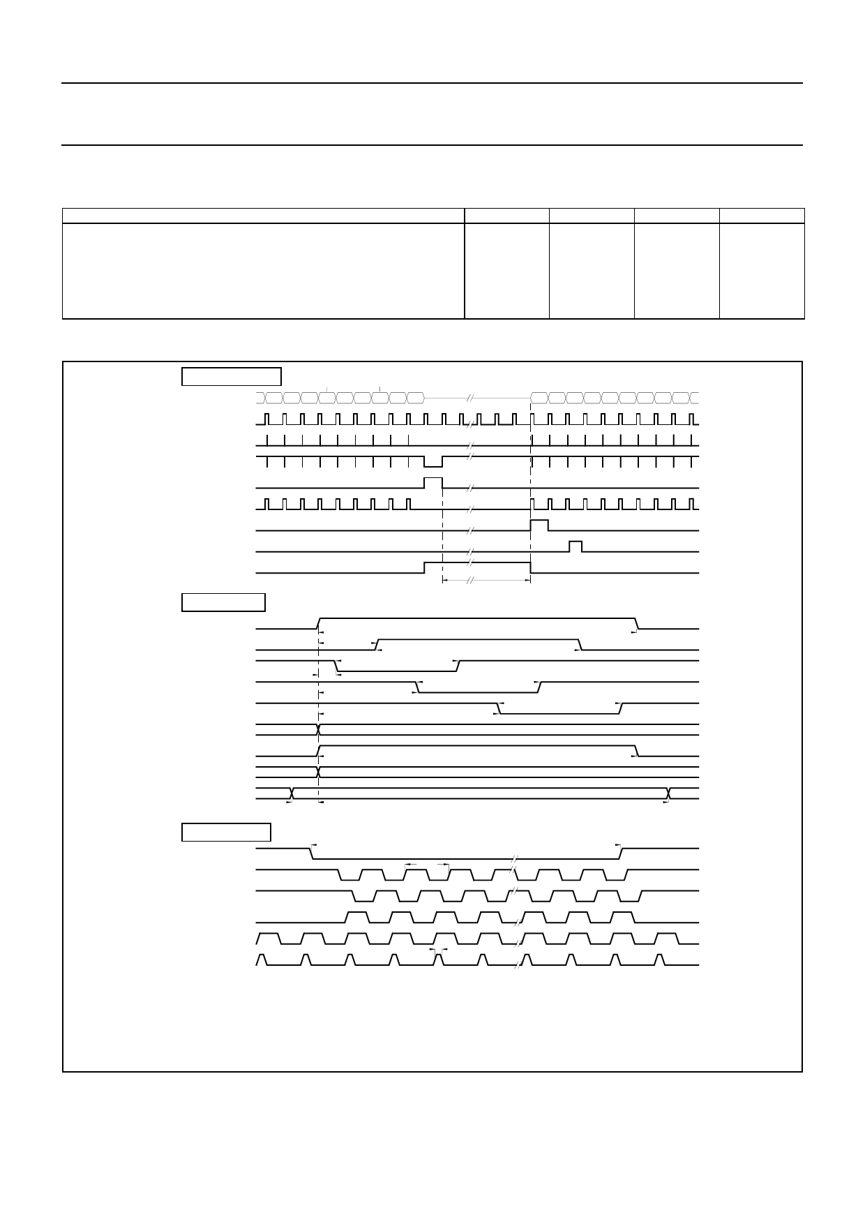
Timing diagrams (for default operation)
AC CHARACTERISTICS
Horizontal frequency (1/Tp) 1
Vertical frequency
Charge Reset (CR) time
Rise and fall times: image clocks (A)
register clocks (C)2
summing gate (SG)
reset gate (RG)
1 Tp = 1 clock period
2 Duty cycle = 50% and phase shift of the C clocks is 120 degrees.
MIN.
10
10
3
3
3
TYPICAL
18
50
193.7
20
5
5
5
MAX.
36
100
1/6 Tp
1/6 Tp
1/6 Tp
Frame Timing
Dummy
Black
Sensor Output
2046 2047 2048 D B B B B B
H
SSC
L
H
A1
L
H
A2, A3, A4
L
H
CR
L
H
Ahigh*
L
H
VD
L
H
BLC
L
H
EXT. SHUTTER L
Line Timing
H
SSC
L
H
A1
L
H
A2
L
H
A3
L
H
A4
L
H
CR
L
H
AHigh*
L
H
VD
L
H
BLC
L
20 Tp
30 Tp
66 Tp
138 Tp
112Tp
204Tp
BBBBBD1 2 3
Integration Time
360 Tp
230 Tp
138 Tp
138 Tp
360 Tp
396 Tp
Pixel Timing
H
SSC
L
H
C1
L
H
C2
L
H
C3
L
H
SG
L
H
RG
L
3127 pixels
1Tp
Tp / 6
Tp = 1 / 18MHz = 55.56ns
Pixel output sequence: 7 dummy, 20 black, 4 timing, 3072 active, 4 timing, 20 black
Line Time: 3487 x Tp = 193.7µs
* During AHigh = H the phiA high level is increased from 10V to 14V (This is necessary during readout only)
VD: Frame pulse
CR: Charge Reset
BLC: Black Level Clamp
A1 to A4: Vertical image clocks
C1 to C3: Horizontal register clocks
SSC: Start-Stop C-clocks
SG: Summing gate
RG: Reset gate
Figure 3 - Timing diagrams
UNIT
MHz
kHz
µs
ns
ns
ns
ns
1999 November
6
Share Link: 