CXA1702AR データシートの表示(PDF) - Sony Semiconductor
部品番号
コンポーネント説明
メーカー
CXA1702AR Datasheet PDF : 24 Pages
| |||
CXA1702AR
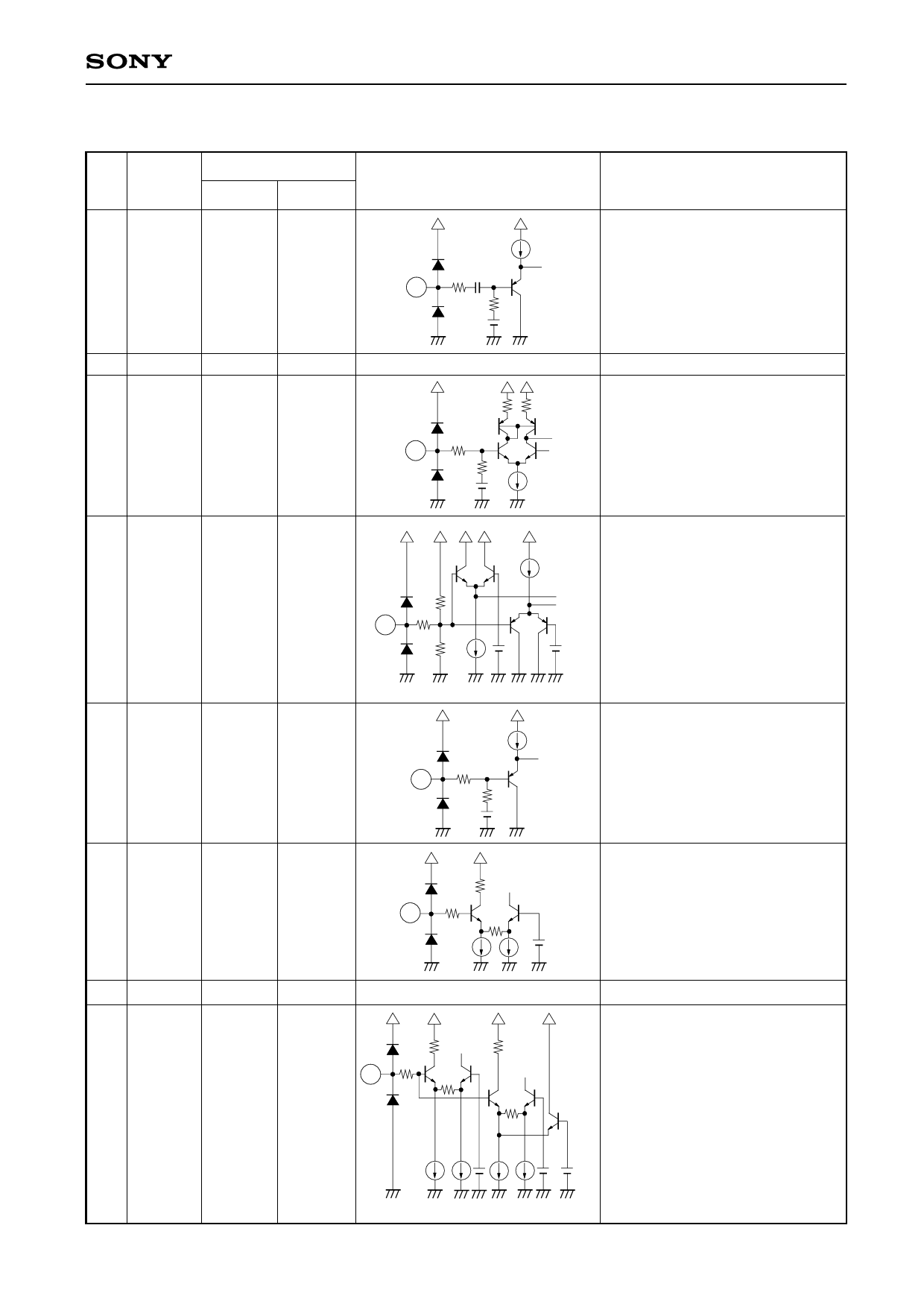
Pin Description
Pin
Symbol
No.
1 AFM IN
Pin voltage
DC
AC
— 125mVp-p
input
(VCC, VCC2, VCC1CH, VCC2CH=4.75V, Ta=25°C)
Equivalent circuit
70µ
20p
1
140
50k
2.45V
Description
Input pin for recording AFM
signal. Input signal bias should
be in the range from 1 V to 3.5 V.
Connect to Vcc when the pin is
not in use.
2 GND2
3 CIN
0V
2.45V
—
500mVp-p
input
3
140
50k
2.45V
25µ
GND pin
Input pin for recording chroma
signal.
4 XDECK 2.4V
—
(when pin
is open)
H: 4.3 V
or more
L: 0.6 V
or less
input
5 YIN
2.45V 500mVp-p
input
20µ
100k
4
140
20µ
100k
2.9V
1.8V
DECK and NORM switching pin
H : NORM (4ch)
} L :
DECK (2ch)
Open :
Input pin for recording Y signal.
40µ
5
140
50k
2.45V
6 LOW 1.8V to
LEVEL 4.75V
input
7
T1
—
8 YLEV_MTG 1.8V to
4.75V
input
—
EVR adjusting pin for low-band
270
6
140
21k
recording signal (chroma, AFM,
video path ATF, PCM path ATF)
level. Increasing the input
3.15V voltage lowers the signal level.
90µ
90µ
—
—
Test pin. Set the pin open.
—
EVR adjusting pin for recording Y
270
270
8
140
23k
14k
signal level and middle tune boost
amount. Adjusts the former during
recording and the latter during
playback. Increasing the input
voltage lowers recording Y signal
90µ 90µ 3.2V 100µ 100µ
level and boost amount.
2.8V 1.75V
YLEVEL
MTG
—3—
Share Link: 