FVXO-LC53 データシートの表示(PDF) - Fox Electronics
部品番号
コンポーネント説明
メーカー
FVXO-LC53 Datasheet PDF : 15 Pages
| |||
FVXO-LC53 Series
Output Wave Characteristics
Parameters
Differential Output Voltage
Output Offset Voltage
Output Symmetry (See Drawing Below)
Output Enable (PIN # 2) Voltage
Output Disable (PIN # 2) Voltage
Cycle Rise Time (See Drawing Below)
Cycle Fall Time (See Drawing Below)
Symbol
VOD
VOS
VIH
VIL
TR
TF
Condition
0.75 MHz to 1.35 GHz
@ 50% VP-P Level
20%~80%
80%~20%
Maximum Value
(unless otherwise noted)
0.6V Typ.
1.3V Typ.
45% ~ 55%
> 70% VDD
< 30% VDD
400 pS
400 pS
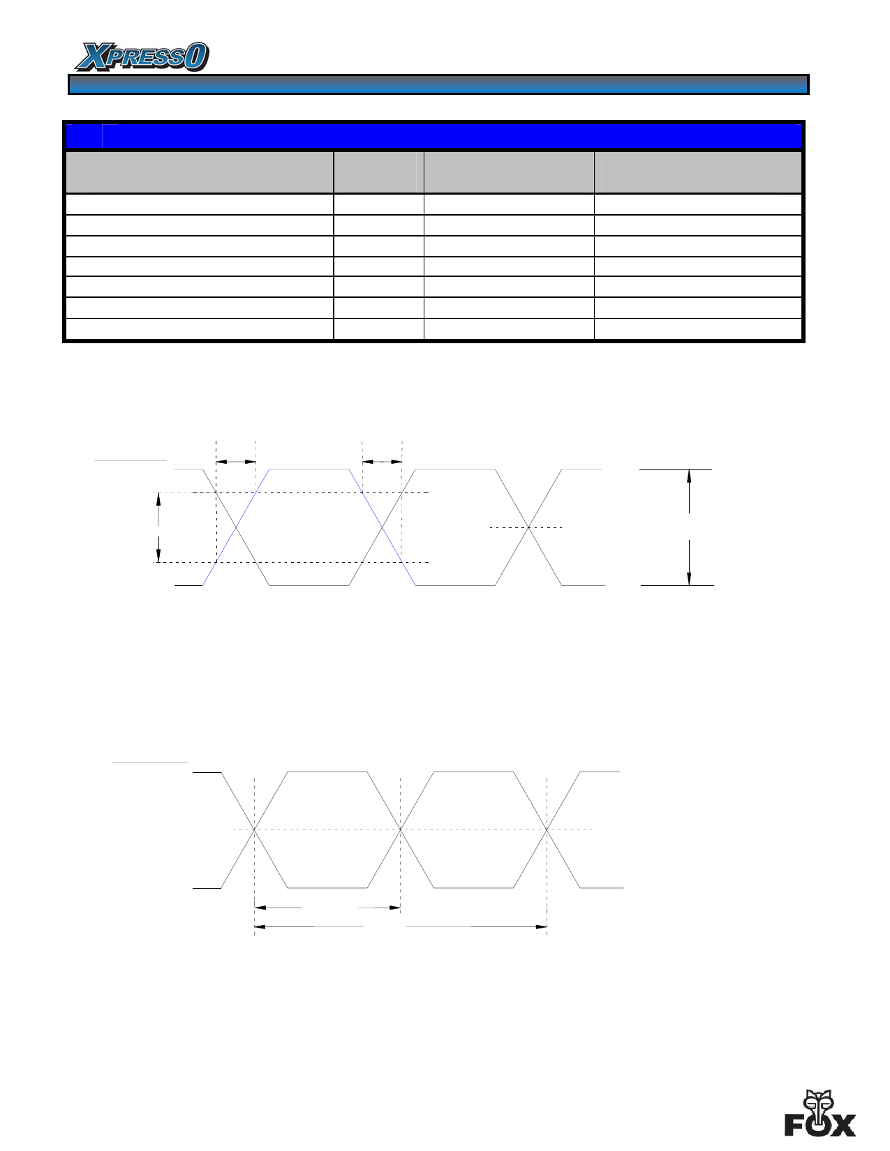
OUTPUT 2
Rise Time / Fall Time Measurements
TR
TF
20% to 80%
50% VP-P
OUTPUT 1
1.30V Typ. 0.6VP-P Typ.
Oscillator Symmetry
Ideally, Symmetry should be 50/50 for 1/2 period -- Other expressions are 45/55 or 55/45
OUTPUT 2
50% VP-P
OUTPUT 1
1/2 Period
Period
Page 4 of 15
© 2008 FOX ELECTRONICS | ISO9001:2000 Certified
Share Link: 