GFP60N03 データシートの表示(PDF) - General Semiconductor
部品番号
コンポーネント説明
メーカー
GFP60N03 Datasheet PDF : 5 Pages
| |||
GFP60N03
N-Channel Enhancement-Mode MOSFET
Electrical Characteristics (TJ = 25°C unless otherwise noted)
Parameter
Symbol
Test Condition
Min
Static
Drain-Source Breakdown Voltage
BVDSS VGS = 0V, ID = 250µA
30
Gate Threshold Voltage
VGS(th) VDS = VGS, ID = 250µA
1.0
Gate-Body Leakage
IGSS
VDS = 0V, VGS = ±20V
Zero Gate Voltage Drain Current
On-State Drain Current(1)
IDSS
VDS = 30V, VGS = 0V
ID(on)
VDS ≥ 5V, VGS = 10V
60
Drain-Source On-State Resistance(1)
Forward Transconductance(1)
RDS(on)
gfs
VGS = 10V, ID = 30A
VGS = 4.5V, ID = 25A
VDS = 10V, ID = 25A
Diode Forward Voltage
Dynamic(1)
VSD
IS = 25A, VGS = 0V
Total Gate Charge
VDS =15V, VGS=5V, ID=50A
Qg
Gate-Source Charge
Gate-Drain Charge
VDS = 15V, VGS = 10V
Qgs
ID = 50A
Qgd
Turn-On Delay Time
Rise Time
Turn-Off Delay Time
Fall Time
td(on)
tr
td(off)
tf
VDD = 15V, RL = 15Ω
ID ≈ 1A, VGEN = 10V
RG = 6Ω
Input Capacitance
Ciss
VGS = 0V
–
Output Capacitance
Coss
VDS = 15V
–
Reverse Transfer Capacitance
Crss
f = 1.0MHZ
–
Source-Drain Reverse Recovery Time
trr
IF = 25A, di/dt = 100A/µs
Note:
(1) Pulse test; pulse width ≤ 300 µs, duty cycle ≤ 2%
Typ
Max
3.0
±100
1
9
11
13
16
40
0.9
1.3
16
22
35
60
8
6
11
20
11
20
48
80
15
30
1850
–
315
–
145
–
160
Unit
V
nA
µA
A
mΩ
S
V
nC
ns
pF
ns
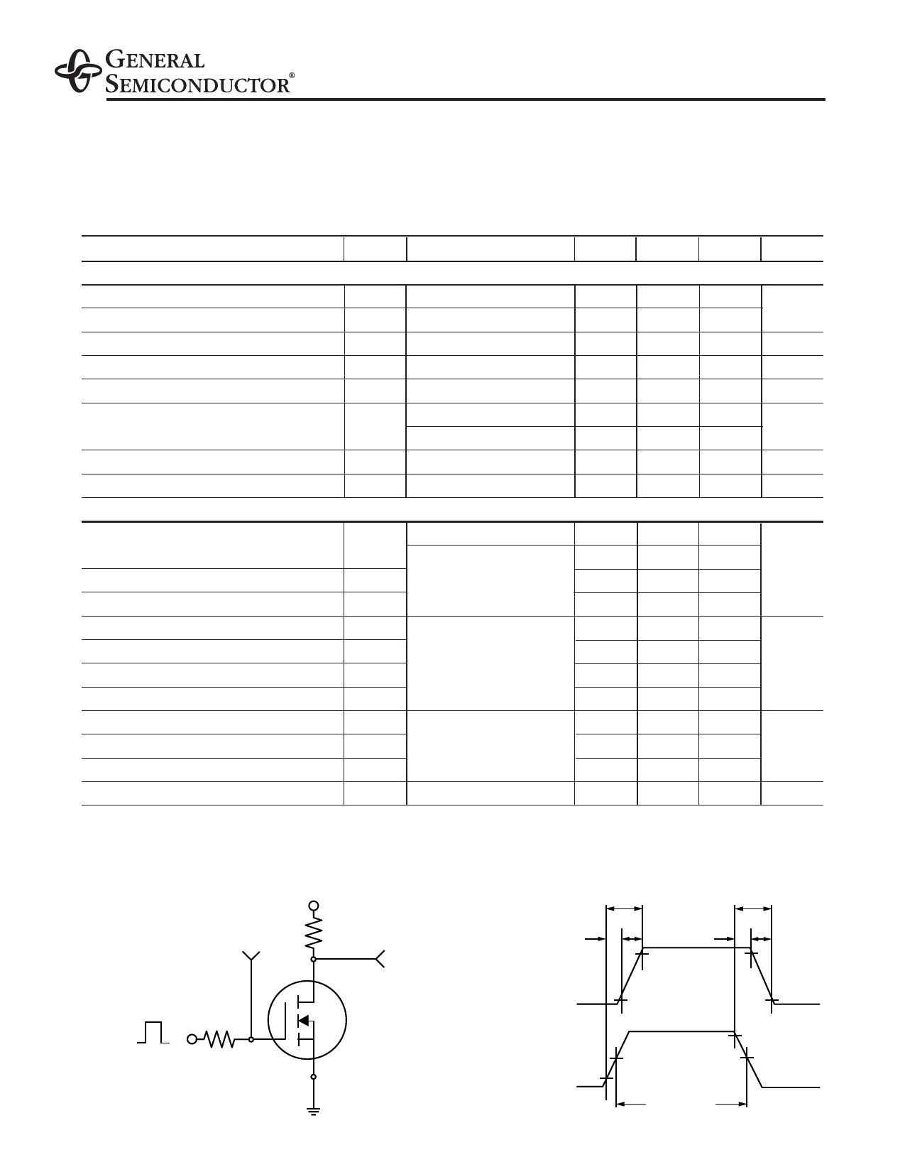
Switching
Test Circuit
VIN
VGEN
RG
G
VDD
RD
D
VOUT
DUT
S
Switching
Waveforms
td(on)
ton
tr
td(off)
90%
toff
tf
90 %
Output, VOUT
Input, VIN 10%
10%
50%
10%
INVERTED
90%
50%
PULSE WIDTH
Share Link: 