GJ1117A データシートの表示(PDF) - Unspecified
部品番号
コンポーネント説明
メーカー
GJ1117A Datasheet PDF : 4 Pages
| |||
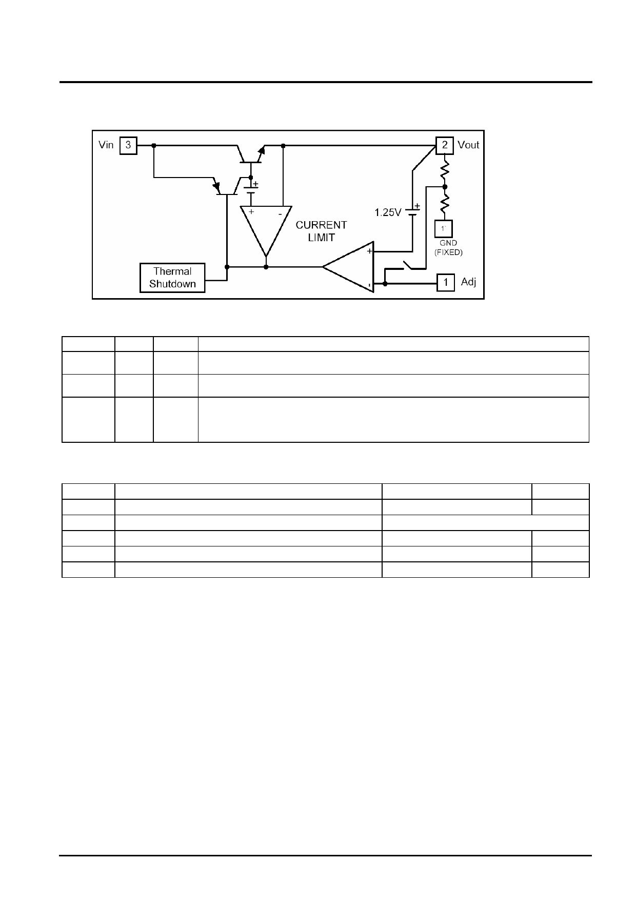
Block Diagram
ISSUED DATE :2003/08/02
REVISED DATE :2006/12/14E
Pin Descriptions
Name I/O Pin#
Adj (GND)
1
Vout
O
2
Vin
I
3
Function
A resistor divider from this pin to the Vout pin and ground sets the output voltage (Ground
only for fixed mode)
The output of the regulator. A minimum of 10uF capacitor must be connected from this pin
to ground to insure stability.
The input pin of regulator. Typically a large storage capacitor is connected from this pin to
ground to insure that the input voltage does not sag below the minimum dropout voltage
during the load transient response. This pin must always be 1.3V higher than Vout in order
for the device to regulate properly.
Absolute Maximum Ratings
Symbol
Parameter
Vin
DC Supply Voltage
PD
Power Dissipation
TST
Storage Temperature
TOP
Operating Junction Temperature Range
TMJ
Maximum Junction Temperature
Ratings
Unit
-0.3 to 12
V
Internally Limited
-65 ~ + 150
к
0 ~ + 125
к
150
к
GJ1117A
Page: 2/4
Share Link: 