LT1959 データシートの表示(PDF) - Linear Technology
部品番号
コンポーネント説明
メーカー
LT1959 Datasheet PDF : 24 Pages
| |||
LT1959
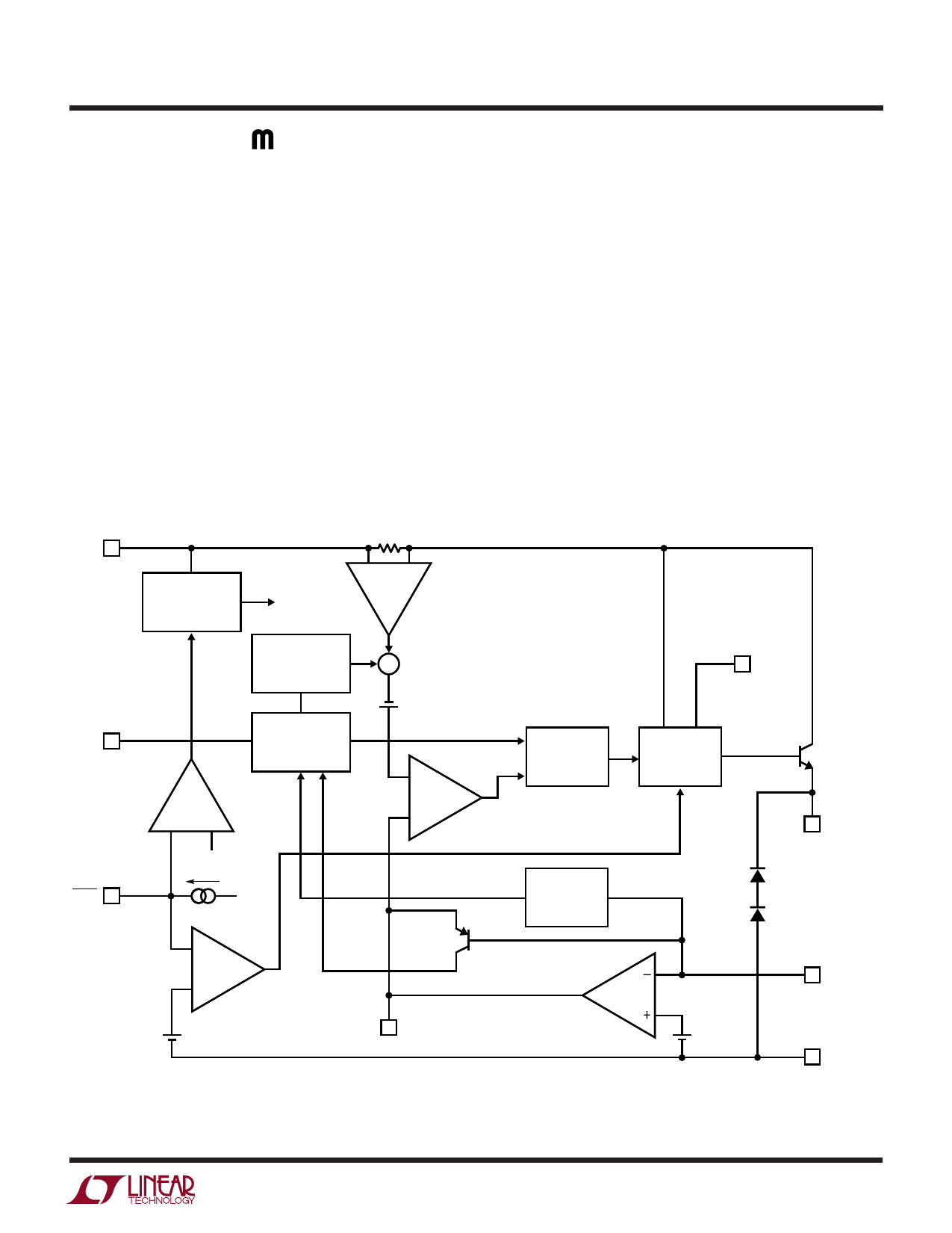
BLOCK DIAGRAM
The LT1959 is a constant frequency, current mode buck
converter. This means that there is an internal clock and
two feedback loops that control the duty cycle of the power
switch. In addition to the normal error amplifier, there is a
current sense amplifier that monitors switch current on a
cycle-by-cycle basis. A switch cycle starts with an oscilla-
tor pulse which sets the RS flip-flop to turn the switch on.
When switch current reaches a level set by the inverting
input of the comparator, the flip-flop is reset and the
switch turns off. Output voltage control is obtained by
using the output of the error amplifier to set the switch
current trip point. This technique means that the error
amplifier commands current to be delivered to the output
rather than voltage. A voltage fed system will have low
phase shift up to the resonant frequency of the inductor
and output capacitor, then an abrupt 180° shift will occur.
The current fed system will have 90° phase shift at a much
lower frequency, but will not have the additional 90° shift
until well beyond the LC resonant frequency. This makes
it much easier to frequency compensate the feedback loop
and also gives much quicker transient response.
High switch efficiency is attained by using the BOOST pin
to provide a voltage to the switch driver which is higher
than the input voltage, allowing switch to be saturated.
This boosted voltage is generated with an external capaci-
tor and diode. Two comparators are connected to the
shutdown pin. One has a 2.38V threshold for undervoltage
lockout and the second has a 0.4V threshold for complete
shutdown.
INPUT
2.9V BIAS
REGULATOR
INTERNAL
VCC
0.01Ω
+–
CURRENT
SENSE
AMPLIFIER
VOLTAGE GAIN = 20
SYNC
SHUTDOWN
COMPARATOR
SLOPE COMP
500kHz
OSCILLATOR
SHDN
0.4V
3.5µA
2.38V
LOCKOUT
COMPARATOR
Σ
0.9V
CURRENT
COMPARATOR
+
S
RS
FLIP-FLOP
R
–
FOLDBACK
CURRENT Q2
LIMIT
CLAMP
FREQUENCY
SHIFT CIRCUIT
ERROR
VC
AMPLIFIER
gm = 2000µMho
Figure 1. Block Diagram
BOOST
DRIVER
CIRCUITRY
Q1
POWER
SWITCH
VSW
PARASITIC DIODES
DO NOT FORWARD BIAS
1.21V
FB
GND
1959 BD
7
Share Link: 