CA3140 データシートの表示(PDF) - Intersil
部品番号
コンポーネント説明
メーカー
CA3140 Datasheet PDF : 22 Pages
| |||

CA3140, CA3140A
RS
120VAC
2
3
7
CA3140
4
30V
NO LOAD
6
RL
LOAD
MT2
MT1
V+
7
2
+HV
LOAD
CA3140
3
4
6
RL
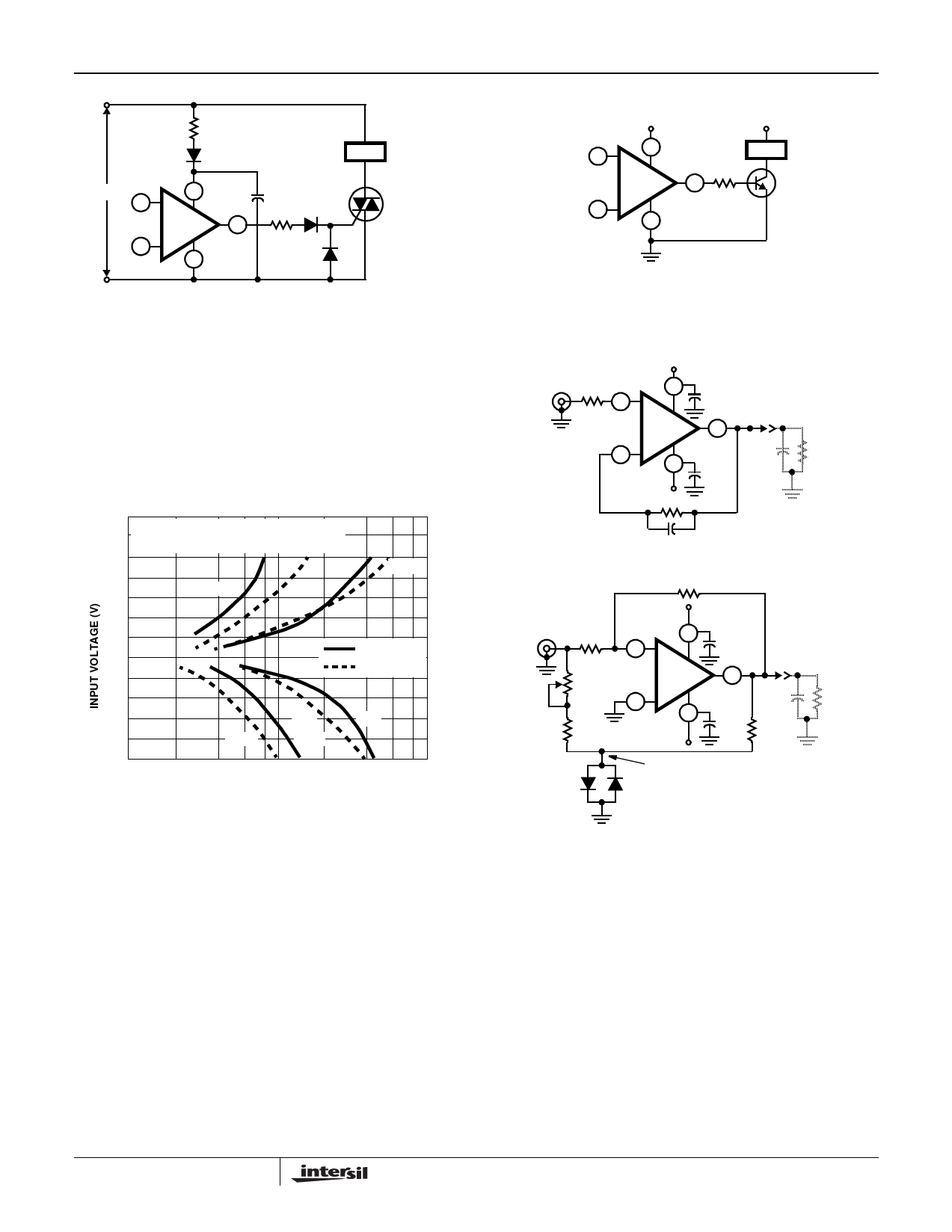
FIGURE 4. METHODS OF UTILIZING THE VCE(SAT) SINKING CURRENT CAPABILITY OF THE CA3140 SERIES
LOAD RESISTANCE (RL) = 2kΩ
LOAD CAPACITANCE (CL) = 100pF
SUPPLY VOLTAGE: VS = ±15V
TA = 25oC
10
8
10mV
10mV
6
1mV
1mV
4
2
FOLLOWER
0
INVERTING
-2
-4
-6
1mV
1mV
-8
10mV
10mV
-10
0.1
1.0
10
SETTLING TIME (µs)
3
10kΩ
2
FOLLOWER
+15V
7
0.1µF
CA3140
6
SIMULATED
LOAD
100pF
2kΩ
4
0.1µF
-15V
2kΩ
0.05µF
INVERTING
5kΩ
+15V
5kΩ
200Ω
4.99kΩ
7
2
0.1µF
CA3140
6
SIMULATED
LOAD
3
100pF
2kΩ
4
0.1µF 5.11kΩ
-15V
D1
1N914
SETTLING POINT
D2
1N914
FIGURE 5A. WAVEFORM
FIGURE 5B. TEST CIRCUITS
FIGURE 5. SETTLING TIME vs INPUT VOLTAGE
Bandwidth and Slew Rate
For those cases where bandwidth reduction is desired, for
example, broadband noise reduction, an external capacitor
connected between Terminals 1 and 8 can reduce the open
loop -3dB bandwidth. The slew rate will, however, also be
proportionally reduced by using this additional capacitor.
Thus, a 20% reduction in bandwidth by this technique will
also reduce the slew rate by about 20%.
Figure 5 shows the typical settling time required to reach
1mV or 10mV of the final value for various levels of large
signal inputs for the voltage follower and inverting unity gain
amplifiers.
The exceptionally fast settling time characteristics are largely
due to the high combination of high gain and wide bandwidth
of the CA3140; as shown in Figure 6.
Input Circuit Considerations
As mentioned previously, the amplifier inputs can be driven
below the Terminal 4 potential, but a series current limiting
resistor is recommended to limit the maximum input terminal
current to less than 1mA to prevent damage to the input
protection circuitry.
Moreover, some current limiting resistance should be
provided between the inverting input and the output when
7