GM317 データシートの表示(PDF) - Gamma Microelectronics Inc.
部品番号
コンポーネント説明
メーカー
GM317 Datasheet PDF : 9 Pages
| |||
GM317
3-TERMINAL 1.5A
ADJUSTABLE REGULATOR
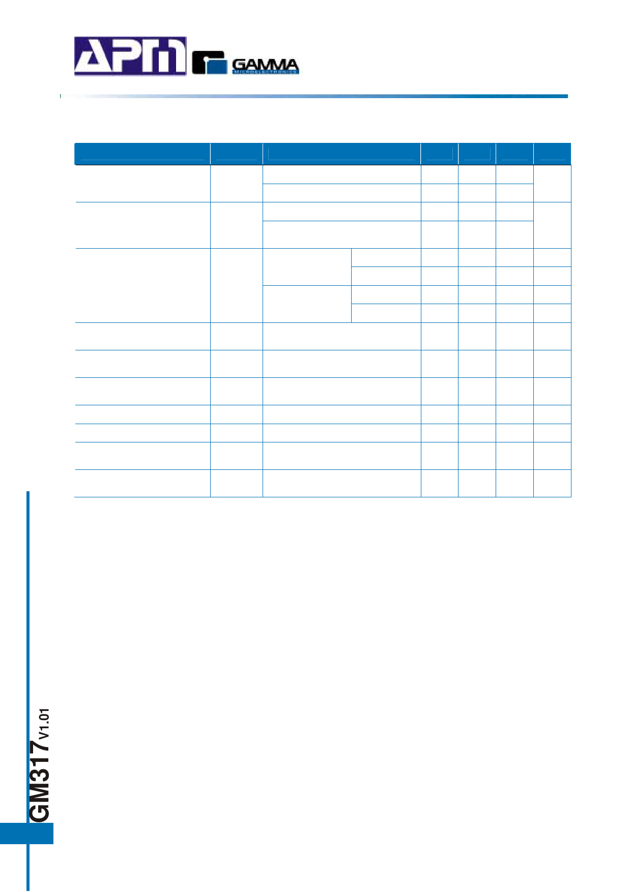
Electrical Characteristics (Unless otherwise noted, VI - VO = 5V and IO= 0.5A. TJ = Full
Range, unless otherwise noted)
Parameter
Symbol
Test Condition
Min Typ Max Unit
Line Regulation (note 2)
Ripple Rejection Ratio
Load regulation (note 3)
Output Voltage Change with
Temperature
Long Term Stability
(Note 4)
∆VOI
∆VOL
∆VOT
3V ≤ VIN – VOUT ≤ 40V, TJ = 25°C
3V ≤ VIN – VOUT ≤ 40V,
VOUT = 10V, f = 120Hz
VOUT = 10V, f = 120Hz, 10µF
capacitor between ADJ and GND
10mA ≤ IOUT ≤ 1.5A, VO ≤ 5V
TJ = 25°C
VO > 5V
10mA ≤ IOUT ≤ 1.2A
VO ≤ 5V
VO > 5V
Full Temperature Range
TJ = 125 OC, VIN – VOUT = 40V,
after 1000hr
0.01 0.04
%/V
0.02 0.07
65
dB
66
80
5
25
mV
0.1 0.5
%
20
70
mV
0.3 1.5
%
%
0.3
1
%
Output Noise Voltage
10Hz ≤ f ≤ 10KHz, TJ = 25°C
0.003
%
Minimum Load Current
Adjustment Pin Current
Adjustment Pin Current
Change
Reference Voltage
IADJ
∆IADJ
VIN – VOUT ≤ 40V
3V ≤ VIN – VOUT ≤ 40V
10mA ≤ IOUT ≤ 1.2A
3V ≤ VIN – VOUT ≤ 40V,
10mA ≤ IOUT ≤ 1.5A, P ≤ 15W
3.5
10
mA
50
100
µA
0.2
5.0
µA
1.2 1.25 1.3
V
Note 1: All characteristics are measured with a 0.1µF capacitor across the input and a 1µF capacitor across the output.
Note 2: Input regulation is expressed here as the percentage change in output voltage per 1V change at the input.
Note 3: Pulse testing techniques are used to maintain the junction temperature as close to the ambient temperature as possible.
Thermal effects must be taken into account separately.
Note 4: Since long-term drift cannot be measured on the individual devices prior to shipment, this specification is not intended to
be a guarantee or warranty. It is an engineering estimate of the average drift to be expected from lot to lot.
4
Share Link: 