GS816272CC-V データシートの表示(PDF) - Giga Semiconductor
部品番号
コンポーネント説明
メーカー
GS816272CC-V Datasheet PDF : 29 Pages
| |||
Preliminary
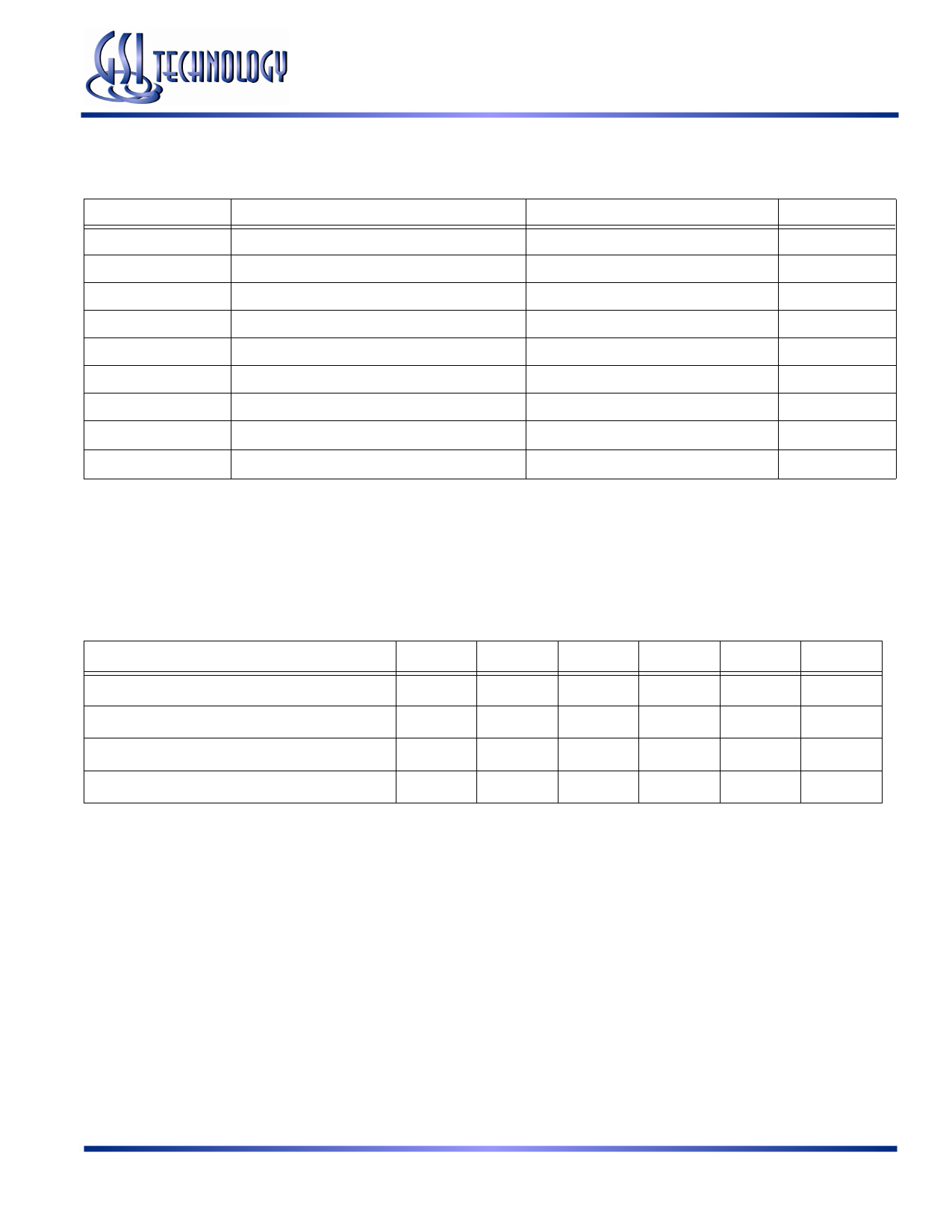
GS816272CC-xxxV
Absolute Maximum Ratings
(All voltages reference to VSS)
Symbol
Description
Value
Unit
VDD
Voltage on VDD Pins
–0.5 to 4.6
V
VDDQ
Voltage on VDDQ Pins
–0.5 to VDD
V
VI/O
Voltage on I/O Pins
–0.5 to VDDQ +0.5 (≤ 4.6 V max.)
V
VIN
Voltage on Other Input Pins
–0.5 to VDD +0.5 (≤ 4.6 V max.)
V
IIN
Input Current on Any Pin
+/–20
mA
IOUT
Output Current on Any I/O Pin
+/–20
mA
PD
Package Power Dissipation
1.5
W
TSTG
Storage Temperature
–55 to 125
oC
TBIAS
Temperature Under Bias
–55 to 125
oC
Note:
Permanent damage to the device may occur if the Absolute Maximum Ratings are exceeded. Operation should be restricted to Recommended
Operating Conditions. Exposure to conditions exceeding the Absolute Maximum Ratings, for an extended period of time, may affect reliability of
this component.
Power Supply Voltage Ranges (1.8 V/2.5 V Version)
Parameter
Symbol Min.
Typ.
Max.
Unit Notes
1.8 V Supply Voltage
VDD1
1.7
1.8
2.0
V
2.5 V Supply Voltage
VDD2
2.3
2.5
2.7
V
1.8 V VDDQ I/O Supply Voltage
VDDQ1
1.7
1.8
VDD
V
2.5 V VDDQ I/O Supply Voltage
VDDQ2
2.3
2.5
VDD
V
Notes:
1. The part numbers of Industrial Temperature Range versions end the character “I”. Unless otherwise noted, all performance specifica-
tions quoted are evaluated for worst case in the temperature range marked on the device.
2. Input Under/overshoot voltage must be –2 V > Vi < VDDn+2 V not to exceed 4.6 V maximum, with a pulse width not to exceed 20% tKC.
Rev: 1.02a 6/2006
10/29
Specifications cited are subject to change without notice. For latest documentation see http://www.gsitechnology.com.
© 2004, GSI Technology
Share Link: 