HD74HC597P データシートの表示(PDF) - Renesas Electronics
部品番号
コンポーネント説明
メーカー
HD74HC597P Datasheet PDF : 10 Pages
| |||
HD74HC597
8-bit Latch / Shift Register
REJ03D0635-0200
(Previous ADE-205-515)
Rev.2.00
Mar 30, 2006
Description
The HD74HC597 consists of an 8-bit storage latch feeding a parallel-in, serial-out 8-bit shift register. Both the storage
register and shift register have positive-edge triggered clocks. The shift register also has direct load (from storage) and
clear inputs.
Features
• High Speed Operation: tpd (SCK to QH’) = 14 ns typ (CL = 50 pF)
• High Output Current: Fanout of 10 LSTTL Loads
• Wide Operating Voltage: VCC = 2 to 6 V
• Low Input Current: 1 µA max
• Low Quiescent Supply Current: ICC (static) = 4 µA max (Ta = 25°C)
• Ordering Information
Part Name
Package Type
Package Code
(Previous Code)
Package
Abbreviation
HD74HC597P
DILP-16 pin
PRDP0016AE-B
P
(DP-16FV)
HD74HC597FPEL SOP-16 pin (JEITA)
PRSP0016DH-B
(FP-16DAV)
FP
PRSP0016DG-A
HD74HC597RPEL SOP-16 pin (JEDEC)
RP
(FP-16DNV)
Note: Please consult the sales office for the above package availability.
Taping Abbreviation
(Quantity)
—
EL (2,000 pcs/reel)
EL (2,500 pcs/reel)
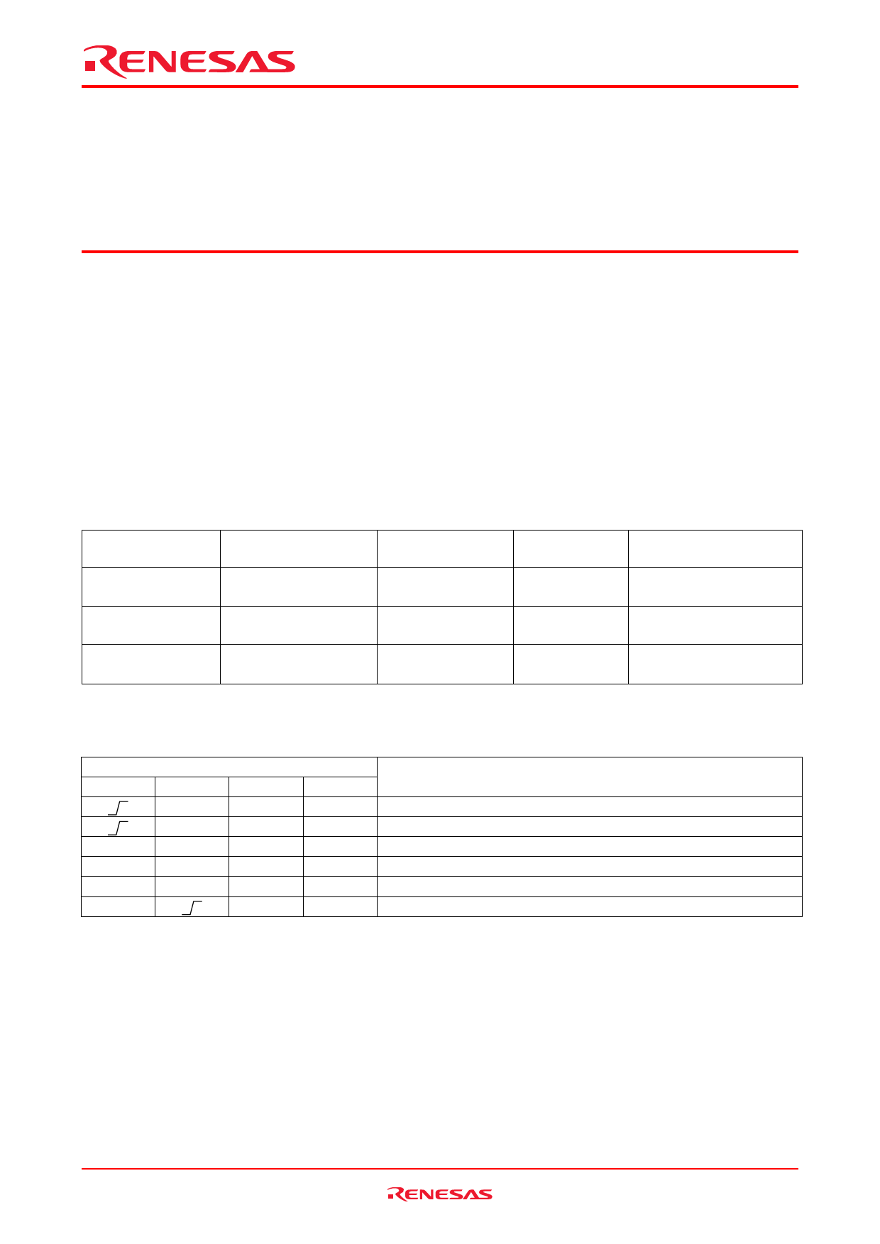
Function Table
RCK
X
X
X
X
Inputs
SCK
SLoad
X
X
X
L
X
L
X
L
X
H
H
SCLR
X
H
H
L
L
H
Function
Data loaded to input latches
Data loaded from inputs to shift register
Data transferred from input latches to shift register
Invalid logic, state of shift register indeterminate when signals removed
Shift register cleared
Shift register clocked Qn = Qn – 1, QA = SER
Rev.2.00 Mar 30, 2006 page 1 of 9
Share Link: 