HD74HCT245FPEL データシートの表示(PDF) - Renesas Electronics
部品番号
コンポーネント説明
メーカー
HD74HCT245FPEL Datasheet PDF : 7 Pages
| |||
HD74HCT245
Electrical Characteristics
Item
Input voltage
Output voltage
Off-state output
current
Input current
Quiescent current
Symbol VCC (V)
VIH 4.5 to 5.5
VIL 4.5 to 5.5
VOH
4.5
4.5
VOL
4.5
4.5
IOZ
5.5
Iin
5.5
ICC
5.5
Ta = 25°C
Min Typ Max
2.0 — —
— — 0.8
4.4 — —
4.18 — —
— — 0.1
— — 0.26
— — ±0.5
— — ±0.1
— — 4.0
Ta = –40 to+85°C
Min Max
2.0
—
—
0.8
4.4
—
4.13
—
—
0.1
—
0.33
—
±5.0
—
±1.0
—
40
Unit
V
V
V
V
µA
µA
µA
Test Conditions
Vin = VIH or VIL IOH = –20 µA
IOH = –6 mA
Vin = VIH or VIL IOL = 20 µA
IOL = 6 mA
Vin = VIH or VIL,
Vout = VCC or GND
Vin = VCC or GND
Vin = VCC or GND, Iout = 0 µA
Switching Characteristics
Item
Symbol VCC (V)
Propagation delay time tPLH
4.5
tPHL
4.5
Output enable time
tZL
4.5
tZH
4.5
Output disable time
tLZ
4.5
tHZ
4.5
Output rise/fall time
tTLH
4.5
tTHL
Input capacitance
Cin
—
Ta = 25°C
Min Typ Max
— 11 22
— 13 22
— 17 30
— 14 30
— 20 30
— 22 30
— 4 12
Ta = –40 to +85°C
Min
Max
—
28
—
28
—
38
—
38
—
38
—
38
—
15
—
5
10
—
10
(CL = 50 pF, Input tr = tf = 6 ns)
Unit
Test Conditions
ns
ns
ns
ns
pF
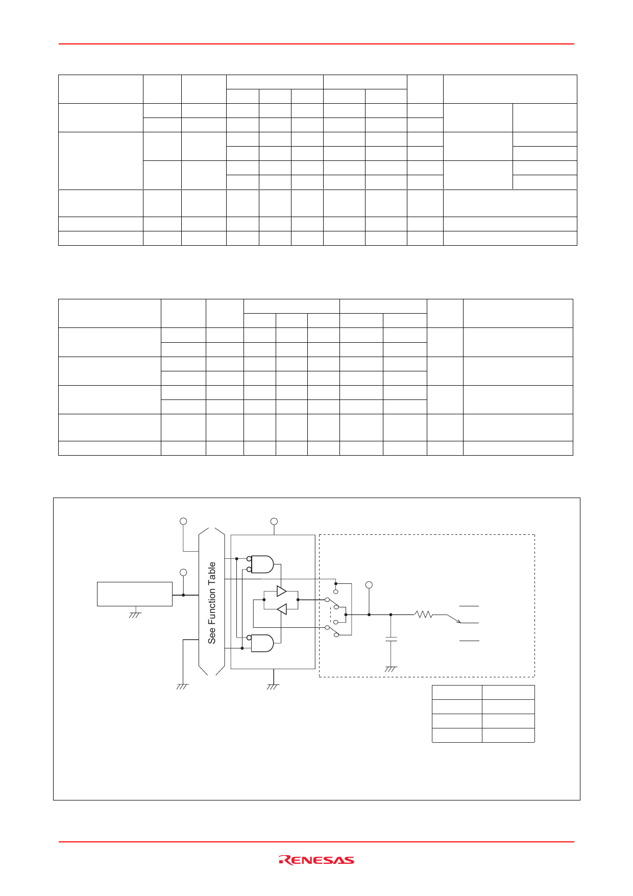
Test Circuit
VCC
VCC
G
Input
Pulse Generator
Zout = 50 Ω
DIR
S1
A1
B1
Output
1 K Ω S2
CL =
50 pF
OPEN
GND
VCC
TEST
tPLH / tPHL
tZH / tHZ
tZL / tLZ
S2
OPEN
GND
VCC
Note : 1. CL includes probe and jig capacitance.
2. A2–B2, A3–B3, A4–B4, A5–B5, A6–B6, A7–B7, A8–B8 are identical to above load circuit.
3. S1 is a input / output swich.
Rev.2.00 Mar 30, 2006 page 3 of 6
Share Link: 